**This is an old revision of the document!**
CMOS manufacturing
Stacked Back-Illuminated CMOS Image Sensor (Bi-CIS)
This page focuses on the process of the tacked Back-Illuminated CMOS Image Sensor (BI-CIS).
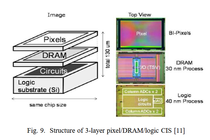
Through SIlicon Vias (TSV)
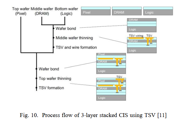
The process flow of stacking the 3-layer CIS is illustrated in the Fig. 10. The fabrication process begins with the par-allel processing of wafers where each wafer is bonded to their respective substrates individually. The DRAM is flipped bonded to the logic substrate face-face. The DRAM substrate is thinned to about 3μm after the bonding. Then, the lower TSVs and the metal wiring connecting both the substrates are formed. Later, the pixel substrate is flipped and bonded to the already stacked DRAM/logic substrate and then the upper TSVs are made to connect the pixel substrate to the rest of the stack