**This is an old revision of the document!**
CMOS manufacturing
Stacked Back-Illuminated CMOS Image Sensor (Bi-CIS)
This page focuses on the process of the tacked Back-Illuminated CMOS Image Sensor (BI-CIS).
MANUFACTURING STEPS
1. Wafer Preparation
Fabrication starts on an epitaxial silicon wafer — a thin, high-purity silicon layer grown on a substrate. The epi layer's thickness and doping are tuned for good light absorption and low crosstalk between neighbouring pixels. The epi thickness has to be thick enough for a good long-wavelength quantum efficiency but thin enough to limit crosstalk and to keep backside thinning practical. The doping purity uniformity of the epi is important to keep metal contamination away from the active photodiode region.
2. Front-end-of-line
FEOL for a CMOS image sensor pixel isn't just “build the transistors” — it's building four specific transistors whose job is to convert a tiny packet of collected charge into a clean, readable voltage : the transfer gate, reset gate, source-follower gate, and row-select gate.
2.1 Well formation
P-wells and n-wells are implanted and thermally driven in to set up the regions where the different transistor types will sit, around the photodiode so the well doping doesn't interfere with the light-collecting region or create unwanted leakage paths to it.
2.1 Well formation
Through SIlicon Vias (TSV)
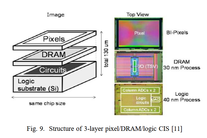
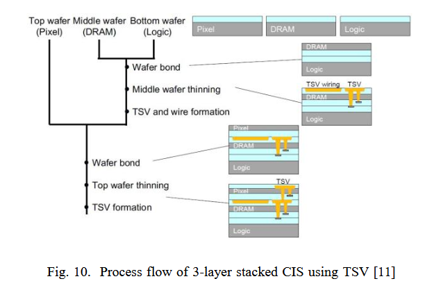
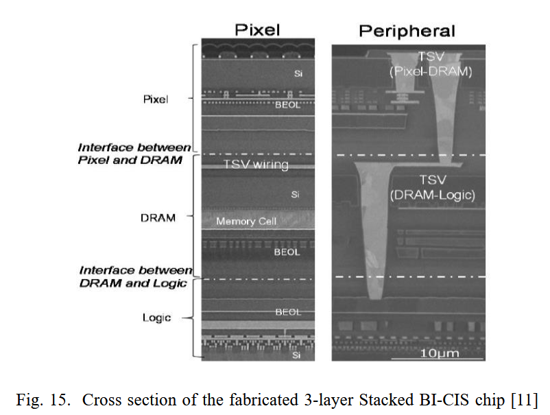
The process flow of stacking the 3-layer CIS is illustrated in the Fig. 10. The fabrication process begins with the par-allel processing of wafers where each wafer is bonded to their respective substrates individually. The DRAM is flipped bonded to the logic substrate face-face. The DRAM substrate is thinned to about 3μm after the bonding. Then, the lower TSVs and the metal wiring connecting both the substrates are formed. Later, the pixel substrate is flipped and bonded to the already stacked DRAM/logic substrate and then the upper TSVs are made to connect the pixel substrate to the rest of the stack
Cu-Cu hybrid bonding
the Cu-Cu bonding process [13], [14] begins with the parallel preparation of wafers Fig. 17(a). A thick dielectric layer is formed on the silicon using the chemical vapor deposition (CVD). CVD is the process of depositing a solid material in vapor form to achieve uniform thickness throughout the surface. Then, the trench and via which are part of the BEOL are made. Using the physical vapor deposition (PVD) method, copper seeds are formed in the trench. Following PVD, the trenches are filled with copper using the electro-chemical deposition (ECD). The excess copper is removed and very low dielectric roughness is attained by chemical mechanical polishing (CMP). Recessing of copper to a certain level is expected during CMP. As seen in 17 (b), the plasma activated wafers are brought together face-to-face and the dielectrics are bonded instantaneously. After CMP, annealing is done at 150°C to 300°C, due to which the metal expands to fill the gap between them. The aforementioned steps confirm that Cu-Cu hybrid bonding provides physical and electrical connections due to the dielectric and metal bonding between the substrates.