**This is an old revision of the document!**
CMOS manufacturing
Stacked Back-Illuminated CMOS Image Sensor (Bi-CIS)
This page focuses on the process of the tacked Back-Illuminated CMOS Image Sensor (BI-CIS).
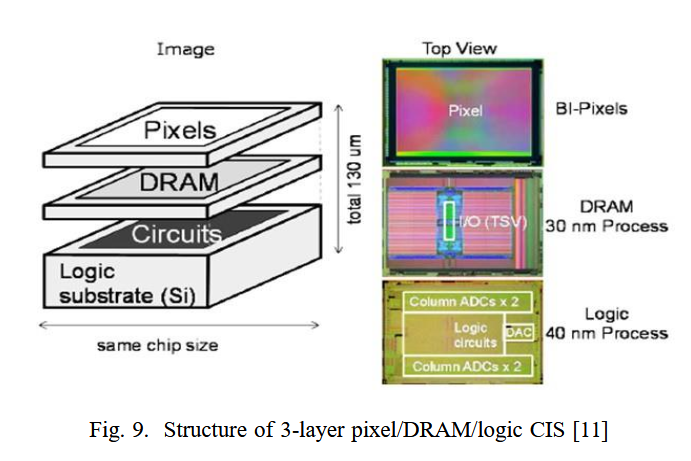
MANUFACTURING STEPS
WORK IN PROGRESS
1. Wafer Preparation
Fabrication starts on an epitaxial silicon wafer — a thin, high-purity silicon layer grown on a substrate. The epi layer's thickness and doping are tuned for good light absorption and low crosstalk between neighbouring pixels. The epi thickness has to be thick enough for a good long-wavelength quantum efficiency but thin enough to limit crosstalk and to keep backside thinning practical. The doping purity uniformity of the epi is important to keep metal contamination away from the active photodiode region.
2. Front-end-of-line
FEOL for a CMOS image sensor pixel isn't just “build the transistors” — it's building four specific transistors whose job is to convert a tiny packet of collected charge into a clean, readable voltage : the transfer gate, reset gate, source-follower gate, and row-select gate.
2.1 Well formation
P-wells and n-wells are implanted and thermally driven in to set up the regions where the different transistor types will sit, around the photodiode so the well doping doesn't interfere with the light-collecting region or create unwanted leakage paths to it.
2.2. Shallow trench isolation
Trenches are etched around the pixel's readout transistors, filled with oxide, and polished flat to electrically separate transistors from each other.
2.3. Gate oxide growth
An extremely thin, uniform oxide layer is grown wherever a transistor channel will form. Its thickness sets the transistor's threshold voltage and switching behavior.
2.4. Polysilicon gate deposition and patterning
A conductive gate layer is deposited over the oxide, then lithographically patterned and etched to define each transistor's exact gate lengt.
2.5. Lightly doped drain (LDD) implants
Light dopant regions are added next to most gate edges to soften the electric field at the drain and improve long-term reliability. The transfer gate is the exception — its doping profile is engineered differently, with a smoother potential slope rather than a sharp LDD junction, specifically to help charge slide cleanly from the photodiode to the floating diffusion instead of getting trapped partway.
2.6. Sidewall spacers
A thin dielectric spacer is formed on the sides of each gate.
2.7. Source/drain implantation
Heavier doping forms the actual source and drain terminals of each transistor. The floating diffusion area is lightly doped, because a smaller floating diffusion electrical capacity means more output voltage per electron collected. A metric called conversion gain that directly determines how much read noise shows up in low light.
2.8. Silicide block
In most logic transistors, a metal silicide is formed on top of the source/drain to cut resistance. Over the photodiode and the floating diffusion, this step is masked off entirely, since silicide formation right next to the light-sensitive node would introduce extra defects and leakage exactly where it matters most.
2.9. Anneal
A final thermal step activates all the implants and repairs the crystal lattice damage from the various implantation steps.
3. Interconnect formation (back-end-of-line)
Multiple layers of metal wiring (copper or aluminum) and dielectric are built up to connect transistors and route signals off the pixel array. In sensors using front-side illumination, this stack sits directly in the light path, so metal routing must be carefully designed to avoid blocking the photodiode.
3.1. Light shields
A metal layer is often deliberately placed as an opaque block over non-photosensitive structures (the floating diffusion, the transistors, and dedicated “dark” reference pixels used for calibration), preventing stray light from generating unwanted charge there.
3.2. Global shutter storage shielding (optional)
Sensors with a global shutter need a charge-storage node shielded almost perfectly from light during readout, since even a tiny light leak would corrupt the stored frame with new photo-charge. This can require dedicated extra metal layers with very high shielding effectiveness.
3.3. Reflective layers
In some BSI designs, a metal layer placed behind the photodiode reflects unabsorbed long-wavelength light back up for a second absorption pass, boosting red/near-infrared sensitivity without needing a thicker silicon layer.
3.4. Final planarization
Because the color filter and microlens sit directly on top of this stack, the last dielectric layer needs to be extremely flat — not just electrically fine, but optically flat across the whole array.
4. Color filter array deposition (TBD)
4.1. Planarization
4.2. Coat resist
4.3. Photoresist exposure
4.4. Develop
4.5. Cure
4.6. Repeat process for each color
4.7. Overcoat
4.8. Inspect
5. Microlens formation
The fabrication methods for microlens arrays are categorized into two primary groups: direct methods and indirect methods 2)
Direct methods
6. Backside illumination (BSI) processing (TBD)
7. Wafer stacking (for advanced sensors) (TBD)
8. Packaging and test (TBD)
Through SIlicon Vias (TSV)
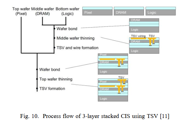
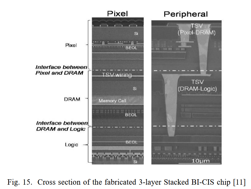
The process flow of stacking the 3-layer CIS is illustrated in the Fig. 10. The fabrication process begins with the par-allel processing of wafers where each wafer is bonded to their respective substrates individually. The DRAM is flipped bonded to the logic substrate face-face. The DRAM substrate is thinned to about 3μm after the bonding. Then, the lower TSVs and the metal wiring connecting both the substrates are formed. Later, the pixel substrate is flipped and bonded to the already stacked DRAM/logic substrate and then the upper TSVs are made to connect the pixel substrate to the rest of the stack
Cu-Cu hybrid bonding
the Cu-Cu bonding process [13], [14] begins with the parallel preparation of wafers Fig. 17(a). A thick dielectric layer is formed on the silicon using the chemical vapor deposition (CVD). CVD is the process of depositing a solid material in vapor form to achieve uniform thickness throughout the surface. Then, the trench and via which are part of the BEOL are made. Using the physical vapor deposition (PVD) method, copper seeds are formed in the trench. Following PVD, the trenches are filled with copper using the electro-chemical deposition (ECD). The excess copper is removed and very low dielectric roughness is attained by chemical mechanical polishing (CMP). Recessing of copper to a certain level is expected during CMP. As seen in 17 (b), the plasma activated wafers are brought together face-to-face and the dielectrics are bonded instantaneously. After CMP, annealing is done at 150°C to 300°C, due to which the metal expands to fill the gap between them. The aforementioned steps confirm that Cu-Cu hybrid bonding provides physical and electrical connections due to the dielectric and metal bonding between the substrates.