**This is an old revision of the document!**
Complementary Metal-Oxide-Semiconductor (CMOS) Image Sensor (⚠️WORK IN PROGRESS⚠️)
Definition
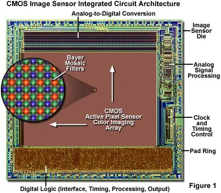
A CMOS sensor (Complementary Metal-Oxide-Semiconductor sensor) is an electronic image sensor that converts light into digital signals using the photodetector principle. Photons are captured and converted into electrons by the photodiode, which are then converted to voltage. An analog-to-digital converter (ADC) then converts this analog information to digital information, which is further processed to create the final image. This technology is used in most modern digital cameras, smartphones, webcams and many scientific imaging devices1).

Main components
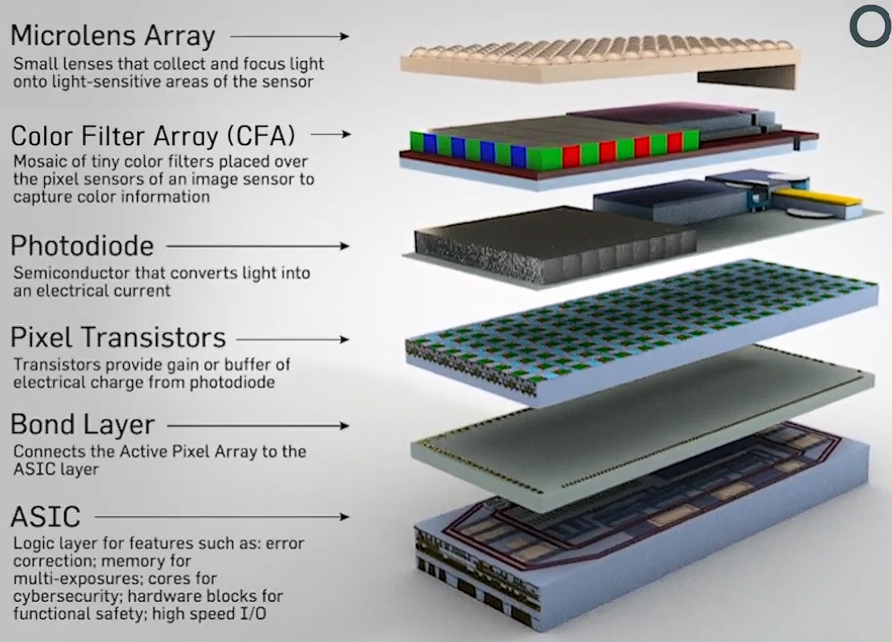
Microlens
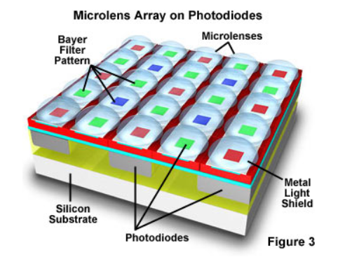
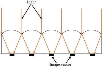
A microlens array is a layer of tiny lenses positioned above the pixels of an image sensor. Each microlens is aligned with a single pixel and concentrates the incoming light onto the photodiode, which is the light-sensitive region of the pixel.
Photodiode
There is three types of vertical photodiodes suitable for fabrication in standard N-well CMOS processes : photodiodes using the N-well/P-sub, P+/N-well, and N+/P-sub junctions.
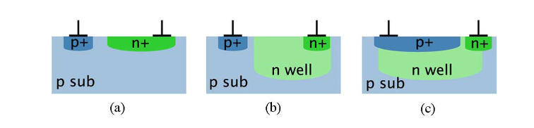
The best type of junction depends on the CMOS structure 7) :
- for 0.7 $\mu$m CMOS process : N+/P-sub
- for 0.35 $\mu$m CMOS process : N-well/P-sub
- for 0.18 $\mu$m CMOS process : P+/N-well
The most-used type of photodiode for CMOS is the pinned photodiiode. 8) The pinned photodiode has a p+/n-well/p-sub architecture, with a 4T pixel structure.
Potential well
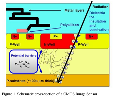
The potential well in a CMOS image sensor is the electron storage region formed inside the N-type pinned photodiode. The combination of the N photodiode and the shallow P+ pinning layer creates a controlled electrostatic minimum that stores photoelectrons with low noise and allows efficient transfer during readout. This structure is the foundation of essentially all modern CMOS image sensors.
The potential well will determine key sensor of the CMOS image sensor such as the Full Well Capacity (FWC), the Charge Transfer Efficiency (CTE), the dark current, the dynamic range, etc.9)
2 main technologies: N-Well and P-Well
N-Well Finished structure : NMOS sits on the P-substrate (left, blue region) PMOS sits inside the N-well (right, pink region) Every terminal : Body, Source, Gate, Drain - is labeled NMOS + PMOS together form one CMOS pair

P-Well Finished structure: PMOS (p+) sits on the N-substrate (dark blue) NMOS (n+) sits inside the P-well (light blue, right) Metal on top connects source, drain, and gate Mirror of the N-well structure — polarity swapped

Working Principle
Photodetector principle
This image shows how a photodector works. The photon penetrates the silicon and create a electron-hole pair connection. The photonic penetration depth on silicon, i.e., the light absorption, depends on the wavelength. This means that the longer the wavelength λ [m] of a photon, the loweris its energy, and the further it can delve into silicon. 12)
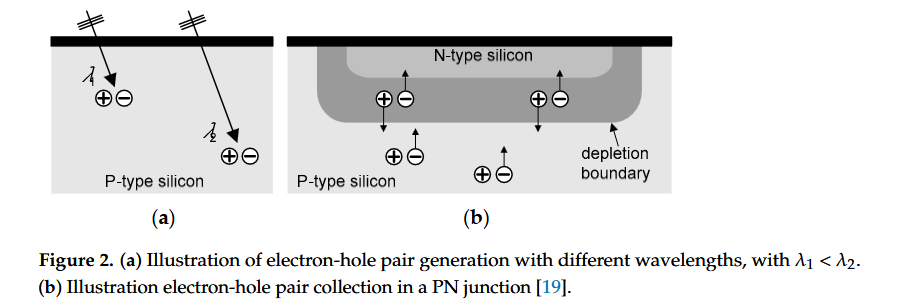
Silicon photodetectors can create photogenerated currents for impinging light with wavelengths across the complete visible range. The produced photocurrent is proportional to the intensity of the incident light and is given by : $$I_{ph} = \frac{e \times QE \times \lambda \times P_i}{hc} = \frac{e \times QE \times P_i}{hv} $$
where Iph [A] is the photocurrent, e [C] is the elementary charge, λ [m] is the wavelength of the incident light, QE [%] is the quantum efficiency, Pi[W] is the incident optical power, h [J.Hz−1] is Plank’s constant, and c [m.s−1] is the velocity of light in a vacuum. The quantity $E = \frac{hc}{\lambda} = h\nu$[eV] is the energy of a photon and ν [Hz] is the frequency of the photons. Formally, the quantum efficiency is determined by the ratio of the generated electrons Ne to the incident photons Nph within the photodetector :
$$QE = \frac{N_e}{N_{ph}} = \frac{\left(\frac{I_{ph}}{e}\right)}{\left(\frac{P_i}{h\nu}\right)} = R \times \left(\frac{h\nu}{e}\right)$$
where R [A/W] is the responsivity of the photodetector. Responsivity is very important because it relates the generated photocurrent Iph [A] with the impinged optical power Pi [W], e.g., R = Iph/Pi [A/W]. Hence, after acquiring the photocurrents, the primary physical quantity that was obtained is the responsivity. Subsequently, the quantum efficiency is derived from Equation (2)
Pixel types
Every pixel includes a photodetector and, depending on architecture, local readout circuitry. Three main architecture: Passive Pixel Sensor (PPS) , Active Pixel Sensor (APS), Digital Pixel Sensor (DPS)

Passive pixel sensor (PPS)
Passive Pixel Sensor (PPS) is a basic CMOS image sensor pixel architecture. Is an early type of digital image sensor. Each pixel uses a photodiode and a single transistor switch to transfer charges without in-pixel amplification.
Active pixel sensor (APS)
Active Pixel Sensor (APS):Each pixel includes active components, typically an amplifier, enabling local charge-to-voltage conversion and multiplexed readout
3T-APS: pixel normally contains a photodiode and three transistors: a reset transistor, a source-follower amplifier, and a row/pixel selection transistor. It operates through three phases 1. Reset transistor 2. Source follower transistor 3. Row-select transistor 4. Photodiode as the light-sensitive element
4T-APS adds a transfer gate and uses a pinned (buried) photodiode instead of a basic p-n junction photodiode. adds one extra transistor compared with 3T APS: 1. Reset transistor 2. Transfer gate 3. Source follower transistor 4. Row-select transistor 5. Pinned photodiode
3T-APS, 4T-APS 16)
 |}}
|}}
Digital pixel sensor (DPS)
Digital Pixel Sensor (DPS) is a CMOS pixel architecture in which analog-to-digital conversion is performed at the pixel level. Each pixel contains a dedicated analog-to-digital converter controlled by reset and select signals. Instead of sending an analog voltage to column circuitry for later conversion, each pixel outputs a digital signal.
Types of illumination
Front side illmunation (FSI) and Bask side illumination (BI)
More for early sensors 18) Since its invention in 1993, CMOS image technology has evolved. The first architectures were front-illuminated, meaning the microlens and color filter were on top, followed by metal wiring for interconnects and the photodiode on the bottom. Since light enters the image sensor through the metal layers, some light information is reflected and lost before reaching the photodiode. This affected the performance of front-illuminated sensors, but Sony Corporation solved the problem by moving the photodiode to the top, next to the color filter. This architecture is known as the back-illuminated (BI) CMOS image sensor, which greatly improved the sensor’s performance.

Stacked Back-Illuminated
Current designs 20) Following the back illuminated sensor, the idea to stack the pixel and the logic circuit sections was proposed to reduce the size of the sensor in the X and Y directions. The pixel section containing the photodiodes was placed on the top and the logic circuitry was moved to the bottom of the architecture on the supporting substrate. This is called the Stacked Back-Illuminated CMOS Image Sensor, which was proposed by Sony Corporation in the year 2012.

Color Filter Array (CFA)
Color filters in CMOS image sensors are necessary because a CMOS photodiode does not naturally detect color. A photodiode mainly converts incoming photons into electrical charge, so by itself it measures only the amount of light, not whether that light is red, green, or blue. To obtain color information, the sensor uses a color filter array, usually called CFA, placed above the pixel array. In the most common Bayer pattern, the filters are arranged as (RGGB) red, green, green, and blue in a 2 × 2 unit. In each color “pixel” consists of a 2-by-2 array of photo-detectors where two are designated to green channel and each of the other two are for the blue and red channels.
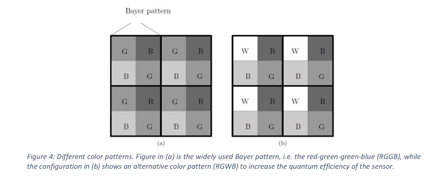

This is useful for color separation, but it reduces quantum efficiency because many photons are rejected before reaching the photodiode. This becomes especially critical in low-light conditions and in small-pixel CMOS sensors, where the photodiode area is already limited. For this reason, one important development is the RGBW or WRGB approach, where a white or clear pixel is added to the color filter array.
Discussion