**This is an old revision of the document!**
Warning: Undefined variable $parcount in /home/clients/973fd5e0710b7a5b5f1f969d927970d7/sites/lib.naknow.eco/lib/plugins/latexcaption/syntax/caption.php on line 121
Warning: Undefined variable $parcount in /home/clients/973fd5e0710b7a5b5f1f969d927970d7/sites/lib.naknow.eco/lib/plugins/latexcaption/syntax/caption.php on line 121
Warning: Undefined variable $parcount in /home/clients/973fd5e0710b7a5b5f1f969d927970d7/sites/lib.naknow.eco/lib/plugins/latexcaption/syntax/caption.php on line 121
Warning: Undefined variable $parcount in /home/clients/973fd5e0710b7a5b5f1f969d927970d7/sites/lib.naknow.eco/lib/plugins/latexcaption/syntax/caption.php on line 121
Warning: Undefined variable $parcount in /home/clients/973fd5e0710b7a5b5f1f969d927970d7/sites/lib.naknow.eco/lib/plugins/latexcaption/syntax/caption.php on line 121
Warning: Undefined variable $parcount in /home/clients/973fd5e0710b7a5b5f1f969d927970d7/sites/lib.naknow.eco/lib/plugins/latexcaption/syntax/caption.php on line 121
Warning: Undefined variable $parcount in /home/clients/973fd5e0710b7a5b5f1f969d927970d7/sites/lib.naknow.eco/lib/plugins/latexcaption/syntax/caption.php on line 121
Warning: Undefined variable $parcount in /home/clients/973fd5e0710b7a5b5f1f969d927970d7/sites/lib.naknow.eco/lib/plugins/latexcaption/syntax/caption.php on line 121
Warning: Undefined variable $parcount in /home/clients/973fd5e0710b7a5b5f1f969d927970d7/sites/lib.naknow.eco/lib/plugins/latexcaption/syntax/caption.php on line 121
Warning: Undefined variable $markup in /home/clients/973fd5e0710b7a5b5f1f969d927970d7/sites/lib.naknow.eco/lib/plugins/latexcaption/syntax/caption.php on line 261
Warning: Undefined variable $markup in /home/clients/973fd5e0710b7a5b5f1f969d927970d7/sites/lib.naknow.eco/lib/plugins/latexcaption/syntax/caption.php on line 261
Warning: Undefined variable $markup in /home/clients/973fd5e0710b7a5b5f1f969d927970d7/sites/lib.naknow.eco/lib/plugins/latexcaption/syntax/caption.php on line 261
Warning: Undefined variable $markup in /home/clients/973fd5e0710b7a5b5f1f969d927970d7/sites/lib.naknow.eco/lib/plugins/latexcaption/syntax/caption.php on line 261
Warning: Undefined variable $markup in /home/clients/973fd5e0710b7a5b5f1f969d927970d7/sites/lib.naknow.eco/lib/plugins/latexcaption/syntax/caption.php on line 261
Warning: Undefined variable $markup in /home/clients/973fd5e0710b7a5b5f1f969d927970d7/sites/lib.naknow.eco/lib/plugins/latexcaption/syntax/caption.php on line 261
Warning: Undefined variable $markup in /home/clients/973fd5e0710b7a5b5f1f969d927970d7/sites/lib.naknow.eco/lib/plugins/latexcaption/syntax/caption.php on line 261
Warning: Undefined variable $markup in /home/clients/973fd5e0710b7a5b5f1f969d927970d7/sites/lib.naknow.eco/lib/plugins/latexcaption/syntax/caption.php on line 261
Warning: Undefined variable $markup in /home/clients/973fd5e0710b7a5b5f1f969d927970d7/sites/lib.naknow.eco/lib/plugins/latexcaption/syntax/caption.php on line 261
Manufacturing processes of multilayer Printed Circuit Boards (PCB)
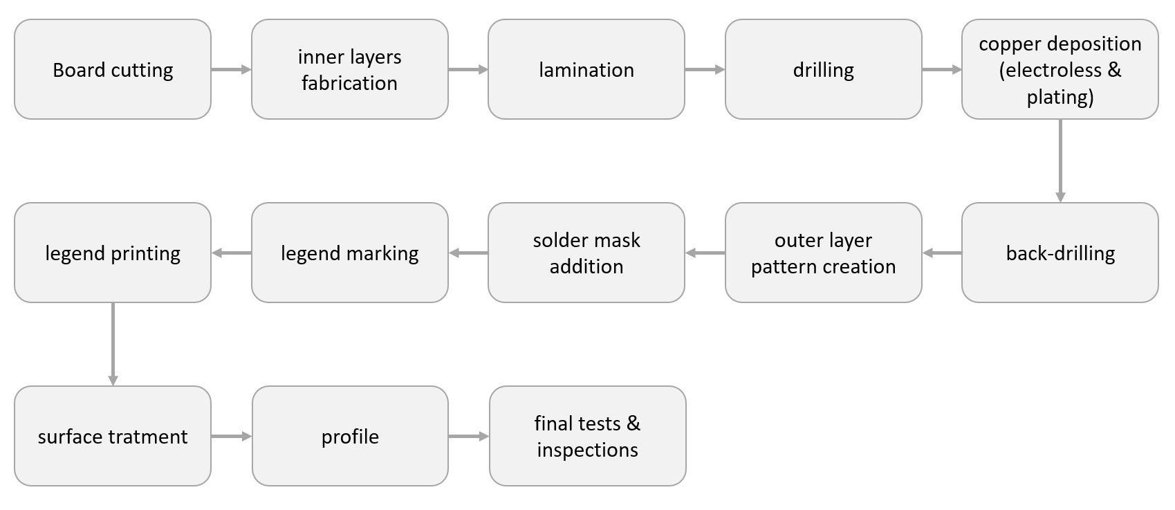
This page aims to explain the manufacturing process flow of multilayer PCB manufacturing. Figure 1 gives an overview of this flow. It is important to note that this flow is adapted depending on the type of PCB (single sided, double sided, or multilayer).
-
1. board cutting
The board is cut and its edges are soften.
-
2. inner layer printing and etching
2.1 pre-treating
During this step the CCL (cooper clade laminate) sheet is cleaned to remove any impurities and to roughned (slighlty) its surface. The roughneing of the surface is important to ensure a good adhesion of the photosensitive film that will be applyied during the next process step. Chemicals (acidic solution) are used for the surface roughening. Once the roughening is done, the board is dryed to stop envenly the roughening process.
2.2. dry photosensitive film lamination
Once the surface is prepared, a photosensitive film is applyied onto the panel. This is done through a lamination machine that laminates a liquid photoresist stucked inbetween two PET and a PE films. The lamination is usually processed in a cleanroom environment (controlled atmosphere and temperature).
2.3. UV ray exposure
During this step the circuit design is transfered onto the photosensitive film. There are two methods to do so:
- exposing all the photosentive film through a mask that has the wanted circuit design,
- by laser direct imaging: the lasers exposes the photosensitive film by drawing the desired pattern that maches the wanted circuitry (no mask is needed).
The panel is now constituted of the CCL sheet on top of which the photosensitive film is polymerised on some areas (the exposed areas), and not polymerised in other areas.
2.4. developpment
In previous steps, specific parts of the resist film have been polimerized through UV light exposure. In this step, the unwanted part of the film (unexposed) will be removed to reveal the copper. It could be either an additive (the exposed part is removed) or a negative (unexposed areas are removed) development. Negative development is the most common method.
2.5. etching
Now that the unwanted copper parts are exposed, it is etched away using amonia or chloride based etchants. The polimerized film is unsensitive to this etching and stays in place to protect some area of panel.
2.6. stripping
In the previous step the unwanted copper has been removed. However the wanted copper is still covered by the polemirized film. This step is focused on removing this resist film by chemically stripping it away. Then, the panel with the desired copper pattern is cleaned to remove remaining stripping chemicals.
3. optical inspection
Optical inspection is processed to check the conformity of the internal layer traces with the virtual design.
4. lamination
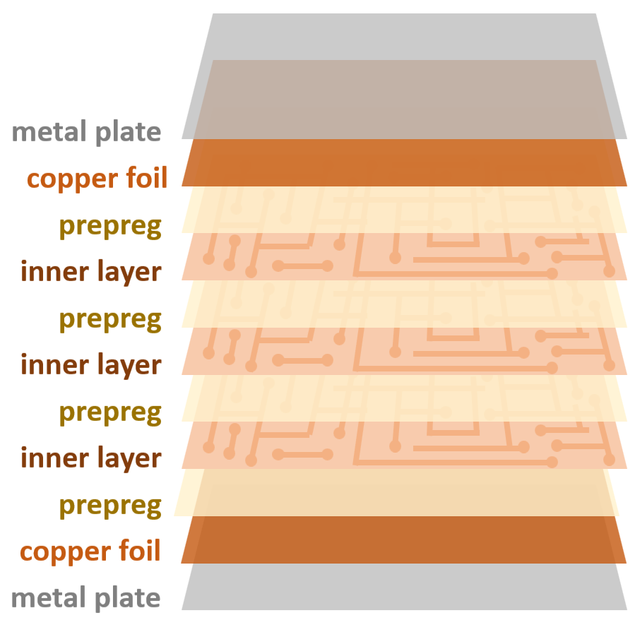
All the inner layers produced previously are assembled together during this process step. Inner layers are superposed one onto another by placing a prepreg sheet intbetween two layers. Prepreg sheet plays the role of a glue.
4.1. Oxidation
The first sub-step is inner layer copper oxidation to prevent its corrosion and to improve adherence with prepreg sheets. To do so, inner layers are cleaned, microetched, the oxide layer is applyied.
4.2. Stacking
Then, all inner layers are stacked using prepreg sheets as a glue inbetween all inner layers. Two steel sheets are used (one on top and one on the bottom) to protect the copper foil layers from damage. These two panels are further taken out of the stack. The stacking-up step is crucial to obtain good quality multilayer PCBs.
4.3. Lamination
This step bonds totgether the different sheets stacked-up previously. The stack is hot-pressed at specific temperatures to melt the resin on each prepreg sheet. Depending on the materials of the panel, the temperature and pressure parameters are adjusted to reach the desired specifications of the panel.
4.4. cooling
Then, the stack goes through a cool-press to prevent any deformation of the panel.
4.5. Drilling position checking
This step is important to allign the innerlayer pattern with outerlayer ones. In this step, X-rays are used to identify the position of the wanted drilling position hat are hidden by the multilayer stack and that shifted a bit during the heat-press due to material deformation.
4.6. edge routing
During this step the excess of copper all around the panel is cutted and the waste is saved for recycling.
4.7. edge milling
TBA
4.8. visual checking
A visual checking is performed to see if the lamination has beeen correctly processed.
5. drilling
The drilling process has several purposes: connect ellectrically all the layers (via hole), attaching components to the PCB (solder through holes), and alligning of the PCB with the final product.
5.1. drilling a location hole
New tooling holes are created to have visible drilling references to align the panel during the next steps of process.
5.2. inserting pins
The panel is placed on top of a base plate to prevent drilling into the machine. The panel is fixed inserting pins into the tooling holes created perviously.
5.3. drilling holes
Holes are drilled controlling the speed and the feeds to avoid any material damage and poor hole quality.
5.4. inspection
An inspection is performed to check is their placement and quality is just as expected.
6. electroless copper deposition
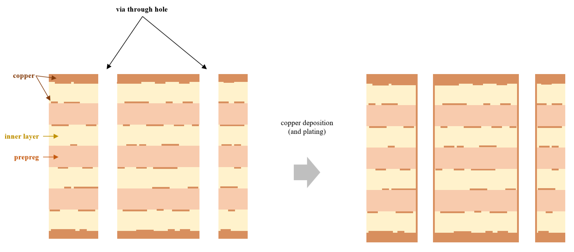
Copper needs to be deposited inside holes to ensure their electrical connection with the rest of the board. To do so, the electroless copper deposition method is used because of its good deposition quality on non-metallic surfaces. Only a small thickness is deposited with this method, the desired thickness will be obtained further in the process flow.
6.1. cleaning
The first step is to chemically clean holes from any residue of the drilling. The board is immerged in the cleaning solution, rinsed and dry.
6.2. activation
The surface is then activated (meaning slightly etched) to enhance the copper deposition.
6.3. copper deposition
Then, the whole panel is immersed in a chemical solution to deposit copper everywhere on the panel and inside holes. The thickness of deposited copper is about 1µm.
7. plating (optional)
More copper needs to be added on the surfce in a thicker layer (about 5-8µm) than what has been done with electroless plating to ensure the required conduction properties of the final product. The galvanic (electrolytic) copper deposition is done vertically.
- Panels are cleaned with acid and rinsed to have a clean surface during deposition.
- The panel is then connected to a cathode and immerged in a solution that is connected to an anode. When applying a current, the copper cations move in the solution to reach the panel: copper is dosited all over the panel surface.
8. back-drilling (optional)
9. outer layer imaging
9.1. Image transfer
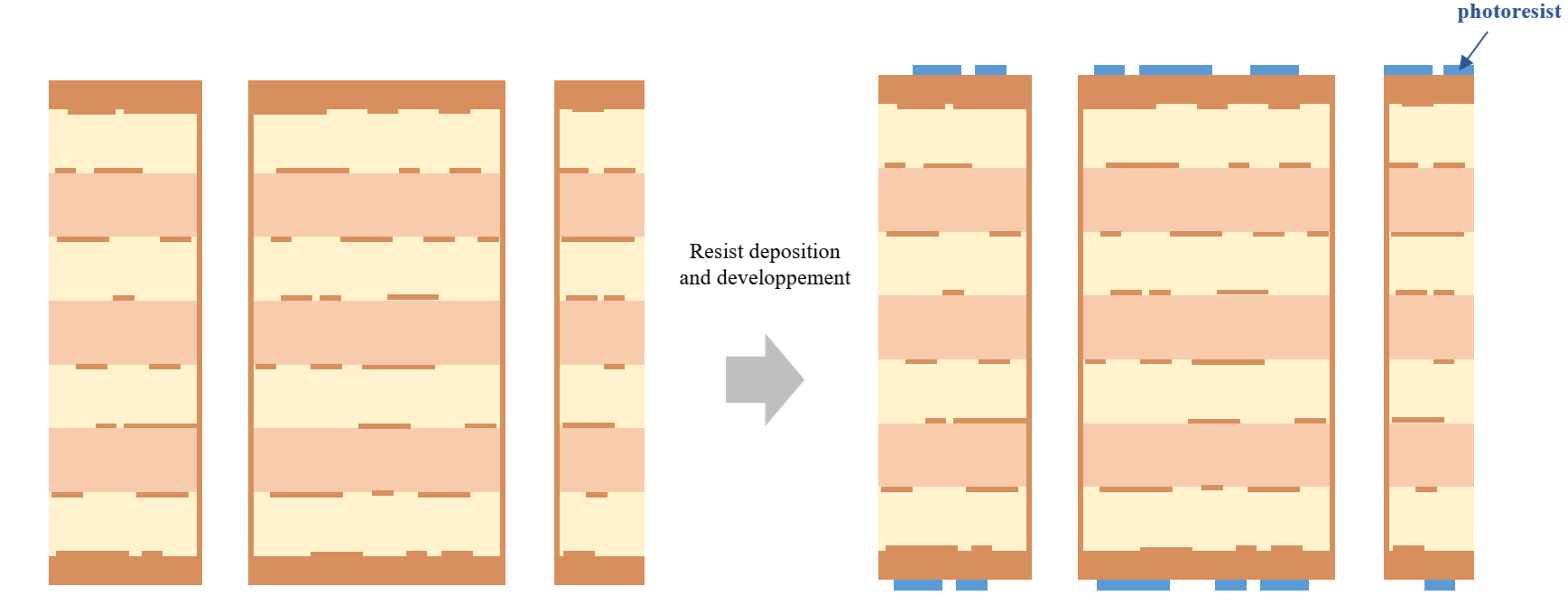
This step is focused on transferring the outer layer pattern on the board to deliver the functionality of the device. The same method as for the inner layer imaging is used (photosensitive film, mask, and UV light). However, in the inner layers the exposed parts were the electrical pattern (the pattern is protected during the following steps)) whereas in the outer layer all the surface of the panel is exposed except for the electrical pattern (in the next step additional copper will be added only on the electrical pattern). Two methods can be used: laser direct imaging (no mask needed), outworks or film and exposing them to UV light. It is crucial to be in a clean room environment because the exposition is very sensitive to any atmosphere change.
9.2. Development
Then the unwanted photoresist is taken out during the developing step, just like the inner layer developing step. The panel is immerged in a chemical solution that reacts with the unexposed the photoresist. The panel is then rinsed to remove any remaining solution composed of chemicals and dissolved photoresist.
10. plating
10.1. copper deposition
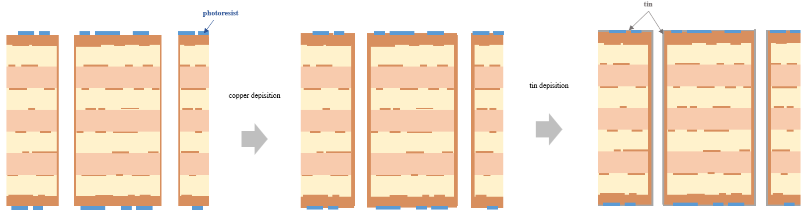
Once the electrical pattern of the outer layer is outlined by the photoresist, an additional copper layer is added to reach the final copper thickness (about 25µm) of the outer layer and inside holes. This additional layer is added if there are some product specifications that go beyond the sanity of the PCB one. Here again the copper deposition is done by the electroplating process.
10.2. tin deposition
Then, to protect the copper in the next process steps a thin tin layer is deposited with the same pattern, here again using the electroplating process (the chemical solution differs from the one used for copper deposition).
11. outer layer etching
11.1. stripping
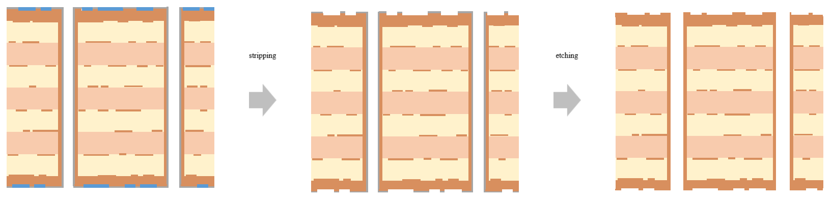
In this process all the remaining photoresist is removed from the panel, outlining the final tin-protected copper design. The resist is chemically removed putting the panel in a chemical solution.
11.2. copper and tin etching
During this step, the remaining photoresist film is stripped away from the panel surface, exposing the copper and tin pattern. Then, etchants are used to remove the unwanted copper (areas where there is no tin). After this step, tin is removed from the panel (with an acid solution) as it was deposited only to protect the final outer layer pattern. To obtain a clean surface, rinsing and drying steps are performed. The PCB is now fully electrically functional.
12. optical inspection
Then the pattern obtained on the panel is scanned and compared to the designed pattern (copper pattern, spacing, etc.).
13. solder mask
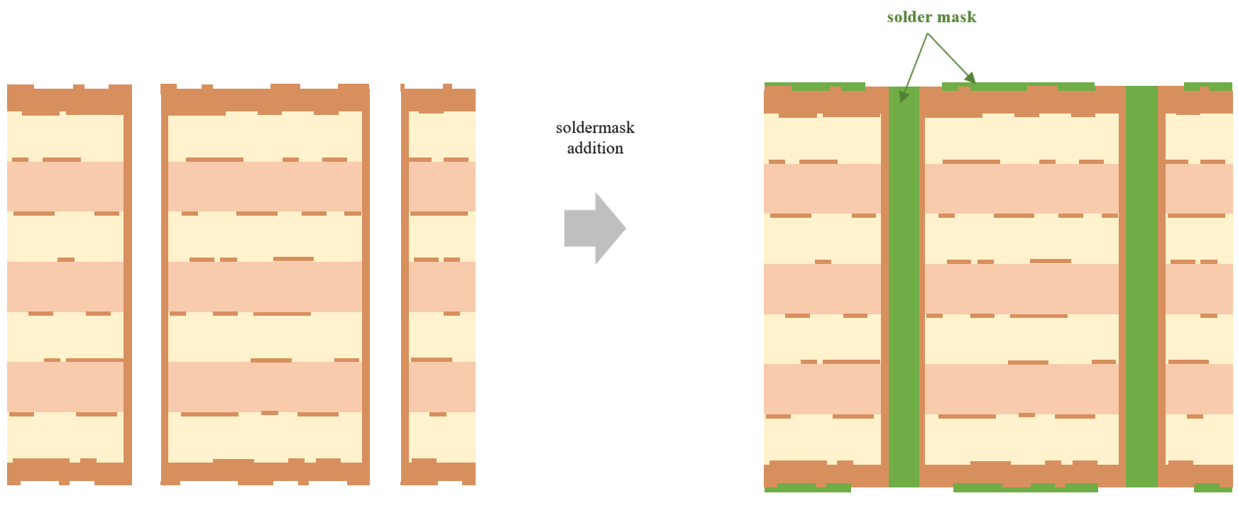
The solder mask is added to protect the metal from oxidation and the pattern from being deteriorated.
13.1. via holes filling
The via holes need to be filled to prevent from any leakage from any chemistry being trapped into the holes during conformal coating processes. A stencil with holes matching the via holes is used: the solder mask (or via plugging ink) is scraped off the stencil so that it lays into the via holes. IPC standards exist to frame the via holes treatment.

13.2. surface coating
The surface is covered to protect areas that needs it (connection of components do not need protection) to prevent oxidations and provide insulation. First, the surface is pumiced (mechanical brushing or chemical etching) to roughened the surface to promote adhesion of the solder mask. The panel is then rinsed and dried to prevent copper corrosion. Then the liquid solder mask is applied on bottom and top surfaces using the stray-coating or a silk screen (one side and then the panel is flipped to conduct the same process on the other side). The solder mask is then hardened by during the pre-cure process so that it stays in place in an even layer.
13.3. solder mask exposure
Now, the panel is ready to be exposed on both sides to UV-light through a mask: the exposure process is very similar to inner and outer layer imaging (other methods exists but this is the most common one). The goal is to make resilient only some part of the solder mask so that only the unwanted solder mask can be later removed.
13.4. solder mask development
Now, the unwanted solder mask can be removed through the development process. The development mixture is sprayed on both sides of the panel and reacts only on the unexposed area. Panels are rinsed and dried to remove the developing solution and the unpolymerized solder mask from both surfaces.
13.5. solder mask checking
Solder mask checking is important to verify its thickness, its adhesion to the board, registration and other elements that may influence quality or reliability.
13.6. solder mask curing
Final curing is needed to fully set the ink. The panel goes into multiple ovens with different temperatures to obtain the full polymerization of the solder mask.
14. legend
Legends are added on the panel to have visual identification of components, factory marks, etc. It can either be processed by inkjet (the ink is applied on the board and then cured to set it) or by negative solder mask printing. In the latter option, the processes are similar to the solder mask addition on the whole panel (the mask design being having the legend pattern).
15. surface finish
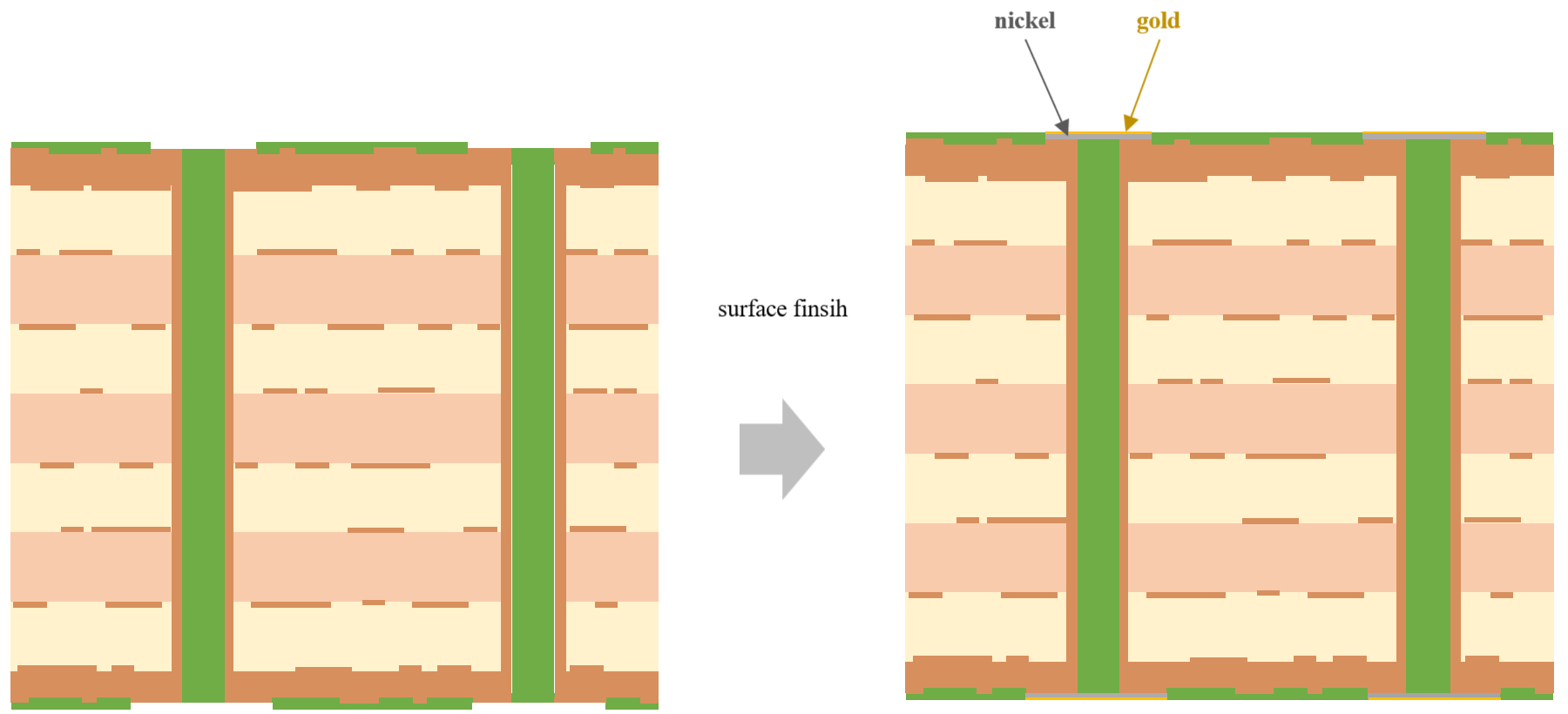
The surface finish can either be ENIG (most common) or tin immersion (often chosen for applications using press fit pins).
Electroless Nickel and Immersion Gold (ENIG)
This step is important because it allows customers to add components to the PCBs and prevents copper oxidation. This process is very complexes. First, the panel goes into a series of chemical bath (a first one – “activator” – to clean and prepare the surface for nickel deposition, the second is an electroless nickel bath, the third one is a immersion gold bath) Gold is applied in a very thin layer (less than 1µm) to protect the nickel from oxidation.
tin immersion
First, the panel undergoes a UV exposure to fully cure the solder mask (if not tin can interact with it), then an acid solution is poured on the surface to clean it and roughened it and chemicals are rinsed out with water. Tin is applied in a very thin layer forming a bond with copper. Then, the PCB is cleaned in warm water and dried. This surface finish is more afordable compared to the ENIG process.
hot air solder levelling (HASL)
This type of surface finish is quite common as the surface is made of a material similar to the one used to solder the components. The first step is to clean to surface. Then, the panel is put into a molted solder bath (with a controlled content of copper): the solder attach itself to copper (which are the areas where solder is needed – other copper areas are covered by the solder mask). Then hot air is blowed onto the surface to remove any excess of solder. The PCB is then cleaned to remove any remaining solder solution.
16. profile
This step is performed to divide the panel in multiple pieces. For instance, usually many PCB are manufactured in one panel, and this step helps separating them from one another.
V-socre
Rotating blade on the upper and lower part of the panel creating a “V-shape” pattern where we want the separation of two PCB to be. The depth of the V-shaped lines is closely controlled.
routing
This is an alternative to V-score process, in which one routing blade follows an outline pattern to separate PCBs. Usually, several panels are process simultaneously by stacking them one on top of another.
17. tests and inspection
electrical test
This step is important to check if the circuit has the right connexions: we are looking for any unexpected short- or open-circuit that would translate a wrong functioning of the PCB. Two method exists to do so: the flying probe test (suitable for smaller volumes and prototypes: each electrical net is tested individually) and the bed of nail or fixture machine (suitable for large batches: all electrical nets are tested simultaneously). The 4-wire kelvin test can also be conducted, in addition of the previous one to check net continuity and resistance.
final inspection
Then each PCB must be inspected to check that there are no remaining defaults in their functioning. Visual checking and and a wide range of other tests are performed to identify any remaining damage on the board.
| Process steps | Process description | Inputs | Outputs |
|---|---|---|---|
| sharp edge removal | soften the edges of the board | CCL sheet (copper sheets + glass fiber impregnated by resin), energy for equipment functionning | |
| cutting | cut the CCL sheet to the required size |
- 2. Inner layer
| Process steps | Process description | Inputs | Outputs |
|---|---|---|---|
| cleaning | remove impurities and increase copper roughness | acidic cleaners, water | acidic cleaners mixed with water |
| drying | blow dry | N2 gas | N2 gas |
| resist film application on the panel | lamination in clean room environment | liquid photoresist on PET film and covered by a PE film, water (+ other chemicals to improve pattern clarity and enhance stability of the film) 1) | N-butyl acrylate and other chemicals |
| resist exposure | exposition of some part of the phooresist through a photomask | UV light 2), photomask (optical-grade quartz or soda-lime glass with sputtered chrome layer, silver-halide emulsion-coated polyester film) | TBA |
| removing unexposed photosensitive film | Potassium carbonate K2CO3 aqueous solution sprayed onto the substrate or sodium carbonate Na2CO3 (the latter one seems the most used one). Or sodium metasilicate Na2SiO3 CAS6834-92-0 3) 4) 5), DI water | ||
| etching | removing the unwanted copper around parts protected by the photosensitive film | amonia or chloride based etchants | TBA |
| stripping | removing remaining photosentsitive film parts | sodium hydroxide solution | TBA |
- 4. Lamination
| Process steps | Process description | Inputs | Outputs |
|---|---|---|---|
| oxidating | roughing and passivating copper | ||
| stacking up | stack up core layers together, copper foil and pre-preg | ||
| laminating | laminating all layers together | Prepreg, Copper foil, Aluminium plate | |
| cooling | |||
| drilling position checking | checking drilling position to avoid misalignment | ||
| edge routing | removing resin or copper foil that sticks out the board | ||
| edge milling | remove rough edges | ||
| visual checking |
- Drilling
| Process steps | Process description | Inputs | Outputs |
|---|---|---|---|
| drilling a location hole | drilling a hole to fix the board for further drilling and ensure allignment | Aluminium sheet, Base sheet | TBA |
| inserting pins | pins to maintain boards together | TBA | TBA |
| drilling holes | Aluminium sheet, Base sheet | TBA | |
| inspection | checking the alignment and the correct position of holes | TBA | TBA |
- electroless copper deposition
| Process steps | Process description | Inputs | Outputs |
|---|---|---|---|
| cleaning | successive steps to remove dust, smear from drilling, etc. | ||
| activation | pepare the surface for plating by modifying its surface properties | ||
| activation | immersing the surface in catalyst colloid to attach it to the surface sites | ||
)
Discussion