
screen_manufacturing
**This is an old revision of the document!**
Table of Contents
Manufacturing processes of Screens
LCD screen manufacturing
OLED screen manufacturing
 manufacturing flow of OLED screen (undetailed)
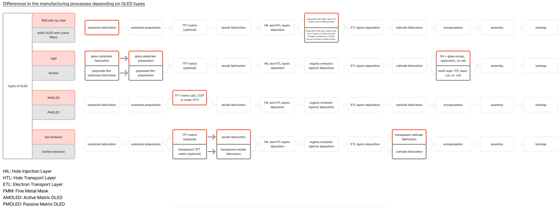
There are multiple process flows depending on the type of OLED that is fabricated.The scheme below lists all the different types of OLED, and how it affects the process flow 1) 2) 3) 4). Each process alternative is explained in the respective section of this page.
}
1. Substrate fabrication and preparation
2. (optional) TFT matrix - only for Active Matrix (AM) displays
 )
)
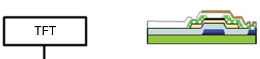
3. (optional) RGB color filter fabrication - only for displays based on white OLEDs
via photolithography 5)
This image shows the red colour filter ony. Red, blue and green colour filters are positioned side-by-side in the pixel.
n
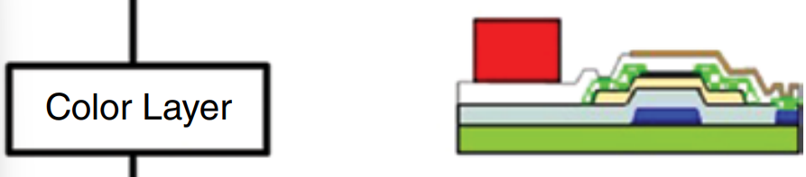
4. Over coat layer
The overcoat layer is formed for three purposes6):
- it prevents any solvent ingredient left on the color layer from diffusing into the OLED layer and deteriorating it during operation
- this layer planarizes the surfaces of the red, green, and blue pixels
- it can work as a white subpixel in WRGB pixel structures. As there is no color filter layer in the white pixels, the empty space is filled with overcoat material, making it a white subpixel, for this reason, the overcoat layer should be thicker than the color layers.
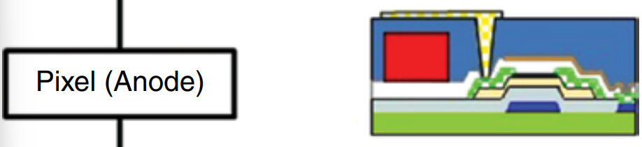
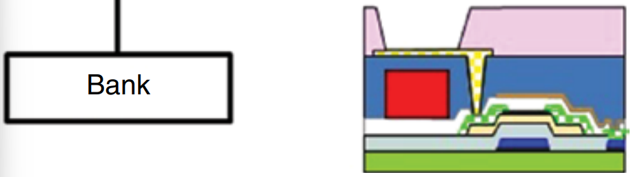
5. pixel fabrication
anode fabrication
bank fabrication
An organic insulator film is used to set apart different colors with a blank layer, and to prevent short circuit between the electrodes. The organic insulator film should be selected among those materials that would not absorb moisture and that show minimum outgassing 7).
cleaning
several possibilites for cleaning treatment: wet8), plasma (e.g.O, N and Ar gases in plasma state)9), UV ozone 10). Plasma treatment show good effectivness 11)
organic material depositions
There are various stacks of material possible, depending on the display size or even on the display performance (brightness, power consumption). A one-stack OLED consists of the superposition of anode, HIL, HTL, EML, ETL, EIL, cathode. A two-stacked OLED consists of two one-stack OLED in series connection. The interconnection layer is called a charge generation layer (CGL) and plays both roles of anode and cathode.
| one stack RGB side-by-side OLED | material |
|---|---|
| cathode | |
| ETL | |
| EML - red&blue&green | |
| HTL | |
| HIL | |
| anode |
| one stack white RGB OLED | material |
|---|---|
| cathode | Al |
| ETL | Mg:Al |
| EML - green | Alq3 |
| CGL | BCP |
| EML - blue&red:dopant | NDP:DCM2 |
| HTL | NPD |
| HIL | none |
| anode | ITO |
| one stack white RGBY OLED | material |
|---|---|
| cathode | Al |
| ETL | NET18:NDN26 |
| HBL | NET18 |
| EML - green:dopant | BH121:GD403 |
| EML - blue:dopant | BH121:EK9 |
| EML - yellow:dopant | HT1:YD3 |
| EML - red:dopant | HT1:RD3 |
| EBL | BH5 |
| HTL | BH5:NDP9 |
| HIL | none |
| anode | ITO |
There are two different deposition methods depending on the size of the display:
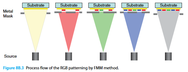
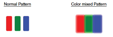
- vacuum thermal evaporation combined with an FMM (Fine Metal Mask)12) - for small sized displays : This method is not selective, meaning the material is deposited everywhere in the equipment chamber : an FMM (Fine Metal Mask) is placed on top of the substrate to hide areas where no material should be deposited. The space between the FMM and the substrate should not be to big to avoid a color mixed pattern. The emissive layer of small display OLEDs consists of 3 emissive materials (respectively emitting red, blue and green light) that are placed side by side. Hence, there are actually 3 successive deposition steps, one for each emissive material as illustrated in the image bellow. The emissive materials are usually organometallic complexes and can be doped or not (e.g.: Alq3 for green and blue phosphorescent light 13), Ir(ppy)3 for phosphorescent green light 14)).
- vacuum thermal evaporation with open mask - for larger sized display: the use of an FMM is not appropriate due to a loss of resolution when the substrate size is increased (there has been a concluant FMM deposition for larger sized screen - 55 inches - but it seems it never reached the production scale).
to be deleted or moved in an other topic. Some notes about the size of the screen and what is considered “small” or “large”. In 2009 LG commercialized a 15-inch OLED TV –> this is nowadays more the size of a laptop screen. When reading article that were written at this period of time we have to be carefull with the adjectives “large” and “small” applied to screen.
HIL (hole injection layer) and HTL (hole transport layer) deposition
TBA
EML (emission layer) deposition
TBA
ETL (electron transport layer) deposition
TBA
cathode fabrication
TBA
6. encapsulation
OLED devices are highly sensitive to moisture and oxygen. They require a water vapour transmission rate (WVTR) of less than 10–6 g/m²/day. For this reason, the encapsulation process is crucial for maintaining a long lifetime. There are multiple encapsulation technologies:

The use of these technologies depends on multiple parameters of the screen.
Frit-seal


This method can't be used for large or flexible screens.
Face-seal


This method is used for large rigid screens.
Thin-Film Encapsulation


This method can be used for flexible screens.
Sources : ([https://www.wiley.com/en-es/Flat+Panel+Display+Manufacturing-p-9781119161363|Flat Panel Display Manufacturing] )
7. assembly
8. testings
1)
Organic light-emitting device and method of manufacturing the same, patent n°US9472767B2, Ja-Hyun Im, Ji-Hwan Yoon, Byung-Hoon Chun, Bum-Suk Kim, 2010
2)
Le guide complet de l'AMOLED Processus de fabrication, Panox Display, 2026
3)
Flat Panel Display Manufacturing, Jun Souk, Shinji Morozumi, Fang-Chen Luo, Ion Bita, 2018
4)
OLED Display Fundamentals and Applications, Takatoshi Tsujimura, 2017
5)
, 6)
Flat Panel Display Manufacturing, p.147, Jun Souk, Shinji Morozumi, Fang-Chen Luo, Ion Bita, 2018
7)
Transmissive Low Outgassing Organic Insulator Suitable for Various OLED Displays, Hiroaki Shindo, Takashi Tsutsumi, Takaaki Sakurai, Masahiro Hanmura, Akira Honma, 2012
8)
Effects of aquaregia treatment of indium–tin–oxide substrates on the behavior of double layered organic light-emitting diodes, F. Li, H. Tang, J. Shinar, O. Resto, S. Z. Weisz, 1997
9)
Surface modification of indium tin oxide by plasma treatment: An effective method to improve the efficiency, brightness, and reliability of organic light emitting devices, C. C. Wu, C. I. Wu, J. C. Sturm, A. Kahn, 1997
10)
Angle dependent X-ray photoemission study on UV-ozone treatments of indium tin oxide, Weijie Song, S.K. So, Daoyuan Wang, Yong Qiu, Lili Cao, 2001
11)
flat panel handbook, p.149
12)
Vacuum Thermal Evaporation for OLEDs: Fundamentals, Optimization, and Implications for Perovskite LEDs, C. Shen, Y. Hu, S. Zhou, et al., 2025
13)
Photoluminescence characteristics of green and blue emitting Alq3 organic molecules in crystals and thin films, Taiju Tsuboi, Yasuko Torii, 2010
screen_manufacturing.1776416886.txt.gz · Last modified: by sophie
Discussion