Manufacturing Process of Screens
Modern flat-panel display manufacture is a highly precise and coordinated operation that involves making ultra-thin, defect-free glass substrates that serves as the foundation for LCD and OLED displays.
Once the glass substrates are ready, the next step depends on the kind of thin film transistor (TFT) backplane technology that is being employed. The TFT backplane acts as the electronic control layer of the display and regulates individual pixels. There are several types of TFT backplanes such as amorphous silicon (a-Si), indium gallium zinc oxide (IGZO), low-temperature polysilicon (LTPS), and low-temperature polyoxide (LTPO).
Glass substrate fabrication
All screen manufacturing processes rely on a glass substrate.
- Fabrication The most common process used in the fabrication of flat glass panels is called the “fusion process.”

Raw materials are mixed, then heated to form molten glass. The molten glass is then refined and conducted to the “isopipe”. The glass overflows its edge, fusing together at the bottom of the isopipe. Molten glass cools and solidifies in midair. It is then cut to form the panel of choice. 1) 2) There are three main companies that produce the majority of glass panels for screens : Corning, Nippon Electric Glass and AGC glass 3)
- Composition
The glass used for flat-panel displays is alkaline earth borosilicate glass. 4) It is composed of Silica (SiO2), Boron trioxide (B2O3), Alumina (Al2O3), and alkaline earth oxides such as Calcium oxide (CaO), Magnesium oxide (MgO), Barium oxide (BaO), Strontium oxide (SrO), Zinc oxide (ZnO), Titanium dioxide (TiO2), Zirconium dioxide (ZrO2). Antimony in the form of Sb2O3 and Arsenic (As2O3) were used as a fining agent, but removed for health issues 5)
LCD screen manufacturing
The TFT LCD is fabricated through four manufacturing blocks include the TFT array process, color filter, liquid crystal cell, module and final testing. The array process mainly focus to build TFT matrix on glass, then it continues to form RGB and electrode during the color filter process. The process then goes through creating liquid crystal cell , then ends with assembly full display.

.
1. Array process
In the TFT array process, the active transistor circuit is created on one glass substrate. It will later control the pixels electrically, and therefore it has the gate lines, data lines, thin-film transistors, storage capacitors, and pixel electrodes. The array process includes glass cleaning, gate metal sputtering, PECVD, photolithography, source/drain etching, and ITO pixel electrode.
Glass Cleaning
Substrate preparation begins with the removal of particles and organic contaminants to prevent pattern defects that lead to yield loss. Cleaning methods are selected based on the surface condition, which include mechanical scrubbing with brushes, high-pressure sprays, UV/plasma cleaning, and rinsing with deionized water (DIW) 6).
Gate Metal Sputtering
Physical Vapor Deposition (PVD) via sputtering is used to deposit a gate electrode layer on the glass substrate. Standard material choices include refractory metals like Chromium (Cr), Molybdenum (Mo), or Aluminum (Al). For high-definition panels, low-resistance metals such as Aluminum or Copper are preferred to minimize signal time-delays. The process occurs in vacuum chambers where magnetic circuits guide ion bombardment to eject metal atoms from a target. Multilayer structures, such as Mo/Al/Mo, are often utilized to improve adhesion and prevent thermal hillocks 7).
PECVD (Plasma-Enhanced Chemical Vapor Deposition)
Plasma-Enhanced Chemical Vapor Deposition (PECVD) is the primary method for depositing the semiconductor and dielectric layers of the transistor. These layers typically include Silicon Nitride (SiNx) for insulation, an intrinsic amorphous silicon (a-Si) channel, and phosphorus-doped n+ a-Si for electrical contacts 8). The process utilizes a parallel plate reactor where precursor gases like Silane and Ammonia are dissociated by plasma. PECVD allows for uniform film quality at the relatively low temperatures required for glass substrates.
Photolithography
This repetitive process transfers precise circuit patterns from a photomask to the thin films deposited on the glass 9). It begins with substrate cleaning to eliminate all contaminants from its surface, Next step involves coating the substrate surface with an adhesion promoter such as hexamethyldisilazane (HMDS), which improves bonding between substrate and photoresist (PR). A photoresist layer is uniformly coated with spinning, which is later on subjected to a pre-bake treatment (soft bake) in order to evaporate solvents and stabilize resist. In the next step, the photoresist is subjected to exposure to ultraviolet radiation using a patterned photomask. There occur chemical changes in the exposed areas of the photoresist. For a positive photoresist, the exposed regions become soluble and are removed during the development process, leaving behind the desired resist pattern. Post-baking (hard bake) is carried out in order to make the remaining photoresist strong and resistant to the upcoming processes. This hardened PR pattern acts as a protective mask during the etching process, where the exposed regions of the underlying thin film are removed10). Finally, the remaining photoresist is stripped away (resist removal), leaving only the patterned thin-film layer on the substrate. Depending on the fabrication process, the patterned photoresist may also serve as a mask for ion implantation or doping instead of etching.
The pixel density of the screen (PPI) determines the pixel size, thus the TFT channel width, finaly imposing a photolitographi size. For exemple, an LTPS IPS LCD screen with a 2K4K resolution, 8“ screen, has a PPI of 550, requires a TFT channel width of 1.5 μm. This was achieved using an i-line (365 nm) photolithography11).

Source/Drain Etching
Etching removes unwanted metal portions to finalize the source and drain electrode patterns. Wet etching is commonly used for materials like Aluminum or Copper due to its lower cost and simple equipment requirements. Dry etching, which uses reactive plasma in a vacuum, provides the higher precision and uniformity needed for high-resolution displays. A single dry etch step can pattern complex multilayer structures like Ti/Al/Ti in one pass. The resulting features are highly sensitive to critical dimension (CD) variations 12). After the metal is removed, the remaining photoresist is stripped away.
ITO Pixel Electrode
Indium Tin Oxide (ITO) is a transparent conductive material sputtered onto the TFT array. It forms the pixel electrode that modulates the liquid crystal while allowing light to pass through the display. ITO is the standard choice for transparent conductors due to its high visible light transmittance and low resistivity 13). Amorphous ITO (a-ITO) is often used during deposition because it is easier to etch without damaging underlying layers. A final thermal annealing step converts the patterned a-ITO into a more stable polycrystalline phase.
2. Color filter process

Black Matrix
Black Matrix (BM) is a light-blocking grid that defines the boundaries of the primary color pixels. It prevents color mixing between sub-pixels and shields the TFTs from ambient light leakage14). BM layers are typically made from carbon-based synthetic resins or Chromium-based multilayers. The resin is coated onto the glass and patterned via standard photolithography. By blocking light between pixels, the BM significantly enhances the display's overall contrast ratio. The effectiveness of this layer is measured by its optical density (OD) value.

Red, Green, and Blue (RGB) Resin Photoresist
These are pigment-dispersed negative photoresists used to form the individual color sub-pixels. Each color layer is sequentially coated, exposed through a mask, developed, and thermally hardened in an oven at approximately 230°C15). Only the areas hardened by light remain on the substrate to form the sub-pixel pattern. Once completed, the entire RGB array is inspected for uniformity and chromaticity.

Overcoat Layer
A transparent overcoat (OC) layer is applied over the finished RGB sub-pixel patterns, with the function to planarize the topographical irregularities caused by varying RGB layer thicknesses. This planarization also ensures a uniform cell gap for the liquid crystal layer. Cross-linked acrylic resins are typically used for this transparent membrane16). The OC also acts as a barrier, preventing organic impurities from the color resins from leaching into the liquid crystal. The layer is hardened through thermal or light-curing methods.
ITO Common Electrode
A continuous transparent electrode is deposited over the color filter or overcoat. In most LCD modes, this common electrode acts as the counter-terminal to the TFT array's pixel electrodes. Indium Tin Oxide (ITO) is standard for this layer because of its high conductivity and optical transparency. In Vertical Alignment (VA) modes, the ITO layer may be patterned with ribs or protrusions to control LC direction17). This electrode provides the necessary electric field to reorient the liquid crystal molecules. For some high-resolution mobile panels, the ITO may be placed on the back side of the glass to prevent static charge buildup.
3. Liquid crystal cell process
PI Alignment Coat
A thin layer of Polyimide (PI) is deposited to the inner surface of TFT and Color Filter substrates. It determines the orientation of liquid crystal molecules. In modern production, instead of roll printing, an inkjet technique for better uniformity and lower consumption is preferred18). The film is initially subjected to a baking process to evaporate solvents, followed by an intensive baking stage at high temperatures. In the end, there is a solid alignment layer resistant to mechanical stress and high temperature. Adequate PI film application ensures good results in terms of display effects depending on different viewing angles.
Rubbing Direction
The PI surface is mechanically rubbed to form micro-grooves determining the alignment of LC molecules. This step involves rubbing the cured PI surface with a velvet-covered roller. LCs orient themselves in accordance with those microgrooves, reducing their internal elastic energy. The strength of the alignment depends on the speed of rotation, depth of rubbing, and the number of rubbing cycles19). The rubbing directions of LCs are carefully chosen according to the switching type of the display. The final step of cleaning eliminates the residues of polymer and dust formed during rubbing.
Seal Printing (ODF)
A sealant resin is dispensed along the edge of the Color Filter substrate. Sealant material used is usually an epoxy and acryl-based resin mixture, which prevent contaminants from entering the liquid crystal display cell20). During the One-Drop Filling (ODF) process, the seal line is placed on one substrate and LC material is dispensed on the other substrate. The dispensing pressure and placement of the nozzle are carefully controlled in order to achieve a small, constant seal width of less than 1mm. Initially, ultraviolet curing is done and afterwards, heat treatment follows.

LC Dispensing
In the One-Drop Filling (ODF) method, precise droplets of liquid crystal are dispensed directly onto the TFT substrate in a vacuum environment. The dropping volume is carefully calculated to avoid defects such as air bubbles. ODF significantly reduces processing time compared to traditional vacuum-filling methods, which could take days for large panels21). Also, the purity of the LC must be maintained to ensure a high voltage holding ratio (VHR) and image stability.
Substrate Bonding
The TFT and Color Filter substrates are aligned and pressed together in a vacuum assembly chamber. Cameras are employed to align the pixels using precise alignment marks at each of the four corners of the glass substrate. It is important that the process is carried out under vacuum conditions since air cannot be allowed to get into the liquid crystal layer when the bonding is done. Pressure is applied to the substrates which are tightly held by the chucks, and they are brought into contact until the desired cell gap is attained.

4. Module process
Polariser Lamination
Flexible linear polariser sheets are attached to the outer surfaces of the assembled LCD cell. These films transmit light of a specific polarization axis while absorbing orthogonal components to modulate display brightness. These polariser films are made from an oriented PVA film containing iodine dye, which is then laminated between two TAC layers. At the very surface, a protective film is applied to avoid any mechanical damage during handling and operation. Below this protective film, there is an additional functional film which can be any type like AG (Anti-Glare), LR (Low Reflection), AR (Anti-Reflection), or HC (Hard-Coat). The back side has an adhesive film that adheres the polariser with LCD cell, whereas a release film covers this adhesive film before installation. It is essential that the direction of polarisation is carefully controlled to align with the direction of orientation of the LC cells.

Module Driver IC Bonding
The Driver ICs are electrically coupled to the panel through Anisotropic Conductive Film (ACF). The chip-on-glass process (COG bonding) is used for small displays, where the IC is directly bonded to the glass substrate. The larger panels use the chip-on-film process, where the IC is bonded to a flexible circuit carrier. ACF comprises micro particles that establish an electrical path between the IC and the panel during heat and pressure application22). Adequate bonding is confirmed by crushing enough particles to ensure adequate electrical paths. Next, silicone resin is applied to the bonded region to offer moisture and corrosion resistance.

PCB Attachment
Printed Circuit Board (PCB) or Flexible Printed Circuit (FPC) is attached to the carrier of driver ICs. This step, usually called “JI”, acts as the crucial link between the device and the video/power signal interface23). ACF is once again employed in the process of bonding the FPC leads to the TFT. The steps involved here include temporary bonding followed by permanent bonding through the use of heated heads. Optical and resistance measurement techniques are adopted to determine alignment and connection of components.
LED Backlight
Since LCDs are non-emissive, they require a Backlight Unit (BLU) to provide uniform illumination. Modern modules use Light-Emitting Diodes (LEDs), which are more efficient and environmentally friendly than older fluorescent lamps. LEDs may be placed along the edges (edge-lit) or in an array directly behind the panel (direct-lit). The BLU produces white light, which the liquid crystal and color filter then modulate to form images24). It is powered and controlled by a dedicated driver or inverter board. Precise matching of the LED spectrum with color filters is necessary to achieve high color saturation.

LGP and Optical Film Assembly
Light from the LEDs enters a Light Guide Plate (LGP) designed to distribute it evenly across the screen area. The LGP uses internal reflection and surface patterns to direct light forward25). Multiple optical films, including diffuser sheets and prism films, are stacked on top of the LGP. Diffusers scatter the light to hide LGP patterns, while prism films collimate the light toward the viewer to enhance brightness. A reflector film is placed underneath the LGP to recycle escaping light. These components are securely held within a plastic module frame.
\ \
OLED screen manufacturing
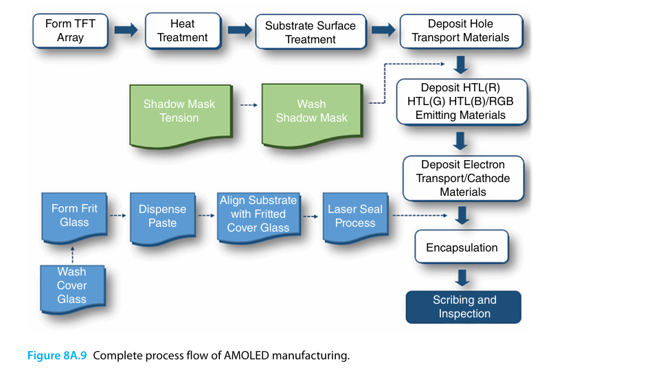
The manufacture of OLEDs comprises five main stages: the production of the pixel control matrix, the production of colour filters (in the case of white OLEDs only), the deposition of the organic materials that make up the OLED, and encapsulation. The sequence of manufacturing stages is illustrated in the Figure 12. The complete process for an AMOLED display is shown in the Figure 13.

There are multiple process flows depending on the type of OLED that is fabricated.The scheme below lists all the different types of OLED, and how it affects the process flow 27), 28),29) , 30). Each process alternative is explained in the respective section of this page.
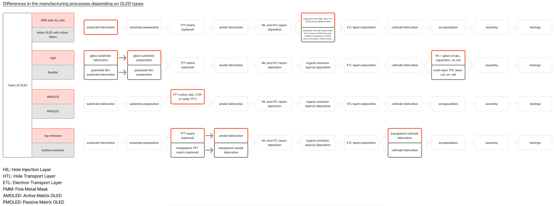
In this section, we chose to focus on the manufacturing processes of the most common OLED screen types. These choices are based on a screen market analysis, detailed in this dedicated page
1. TFT matrix (only for Active Matrix (AM) displays)
For Active Matrix OLED (AMOLED), a TFT matrix matric is constrcucted on the glass substrate. LTPS TFT technology is used for small and medium-sized screens, and IGZO TFT technology for larger ones. These technologies are explained in this section . An AMOLED device needs two TFTs : the switching TFT store the data signal in storage capacitor to provide a voltage without time loss, and the driving TFT delivers current modulated by the signal voltage to the pixel for light emission 31).
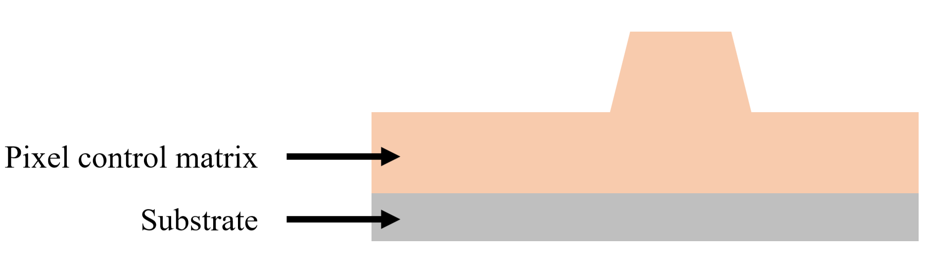
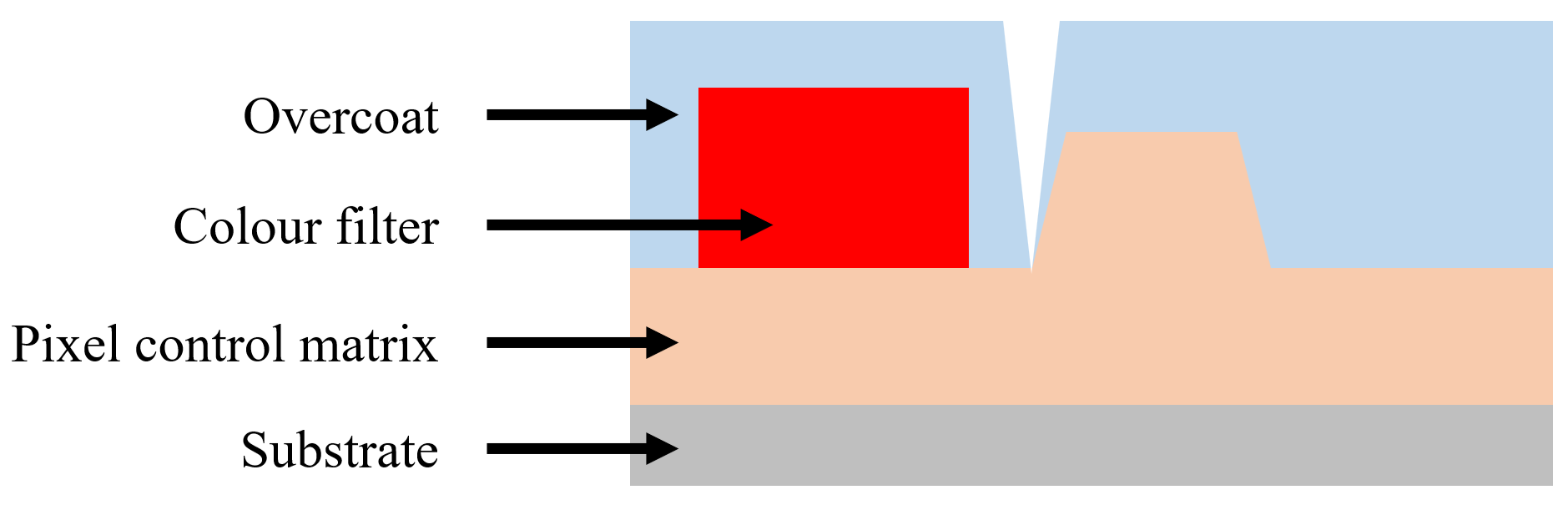
2. Color filter fabrications (only for displays based on white OLED)
via photolithography 33)
This image shows the red colour filter ony. Red, blue and green colour filters are positioned side-by-side in the pixel.
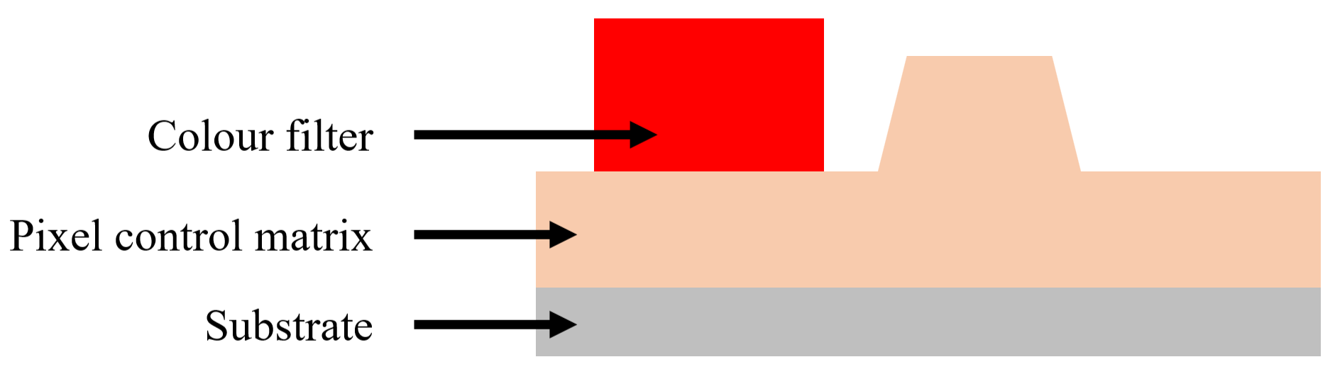
3. Over coat layer
The overcoat layer is formed for three purposes35):
- it prevents any solvent ingredient left on the color layer from diffusing into the OLED layer and deteriorating it during operation
- this layer planarizes the surfaces of the red, green, and blue pixels
- it can work as a white subpixel in WRGB pixel structures. As there is no color filter layer in the white pixels, the empty space is filled with overcoat material, making it a white subpixel, for this reason, the overcoat layer should be thicker than the color layers.
4. Pixel fabrication
Anode fabrication
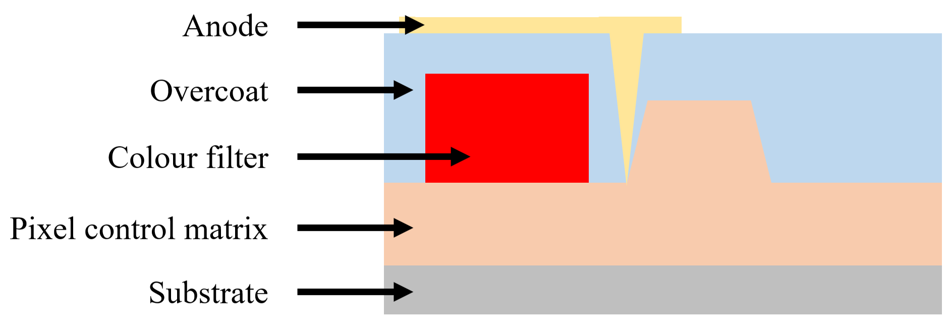
The anode is formed on the substrate and the pixel control circuit. In the case of bottom-emission, the anode must be transparent to allow light to pass through it. Conversely, if the OLED is configured for top-emission, the anode must be reflective. The light passes through the cathode, and the reflective properties of the anode serve primarily to increase the light output efficiency. Figure 18 illustrates the deposition of the anode (coloured in yellow) onto a TFT substrate of a white OLED.
Bank fabrication
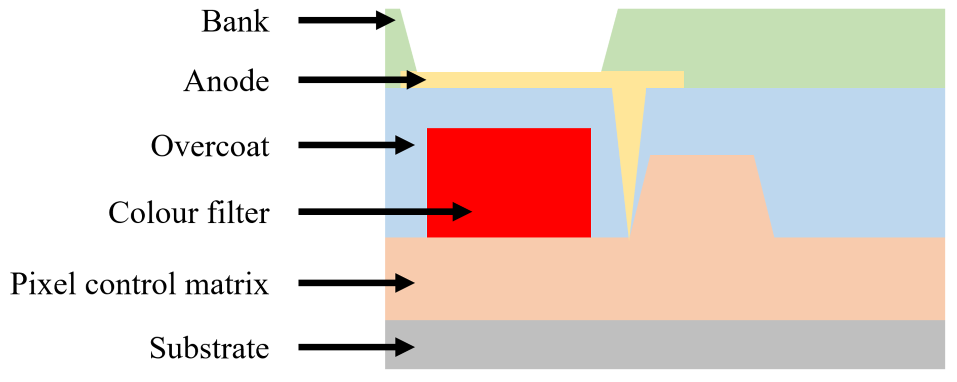
An organic insulator film is used to set apart different colors with a blank layer, and to prevent short circuit between the electrodes. The organic insulator film should be selected among those materials that would not absorb moisture and that show minimum outgassing 38). The figure illustrates the addition of the insulating layer to the anode. Figure 19 illustrates the addition of the insulating layer to the anode during the manufacture of a white OLED.
Cleaning
There are several cleaning treatment: wet40), plasma (e.g.O, N and Ar gases in plasma state)41), UV ozone 42). Plasma treatment show good effectivness 43)
Organic material depositions
There are two different deposition methods depending on the size of the display:
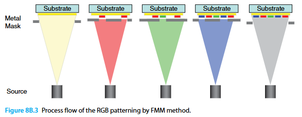
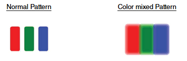
- vacuum thermal evaporation combined with an FMM (Fine Metal Mask)44) - for small sized displays : This method is not selective, meaning the material is deposited everywhere in the equipment chamber : an FMM (Fine Metal Mask) is placed on top of the substrate to hide areas where no material should be deposited. The space between the FMM and the substrate should not be to big to avoid a color mixed pattern. The emissive layer of small display OLEDs consists of 3 emissive materials (respectively emitting red, blue and green light) that are placed side by side. Hence, there are actually 3 successive deposition steps, one for each emissive material as illustrated in the image bellow. The emissive materials are usually organometallic complexes and can be doped or not (e.g.: Alq3 for green and blue phosphorescent light 45), Ir(ppy)3 for phosphorescent green light 46).
- vacuum thermal evaporation with open mask - for larger sized display: the use of an FMM is not appropriate due to a loss of resolution when the substrate size is increased (there has been a concluant FMM deposition for larger sized screen - 55 inches - but it seems it never reached the production scale).
All the materials for the organic layers (HIL, HTL, EML, ETL) are therefore deposited using the methods described above.
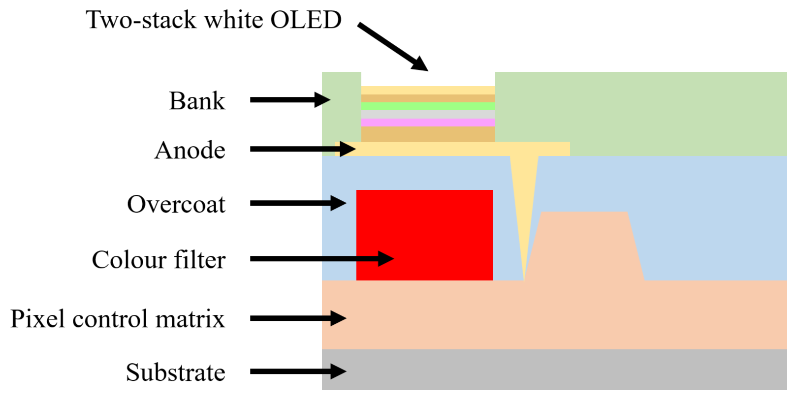
As an example, Figure 22 shows all the layers previously manufactured and the two-stacked white OLED.
Cathode fabrication
The cathode is mostly made of Al or Ag 49) for bottom-emission (it needs to be reflective), and and Mg:Ag 50) for top-emission (semi-transparent).
The processes used for deposition of the cathode are either vacuum thermal evaporation combined with an FMM (Fine Metal Mask)51) for small displays, or vacuum thermal evaporation with open mask for large displays.
5. Encapsulation
OLED devices are highly sensitive to moisture and oxygen. They require a water vapour transmission rate (WVTR) of less than 10–6 g/m²/day. For this reason, the encapsulation process is crucial for maintaining a long lifetime. There are multiple encapsulation technologies:

The use of these technologies depends on multiple parameters of the screen.
Frit-seal
Frit sealing 53) is an encapsulation technology for OLED panels that involves mixing glass/metallic oxide powders with organic binders into a paste, printing it onto glass substrates, then fusing them together using an IR laser.
This process yields outstanding moisture resistance (comparable to glass itself), eliminating the need for separate desiccants or passivation layers. It also enabled “zero gap” technology, thinner panels, reduced Newton ring defects, and narrow bezel designs — making it the dominant OLED encapsulation method for some time.
However, the technology has significant limitations: it is prone to fine cracks during handling, and its inherent brittleness makes it unsuitable for large (over 20 inches) or flexible OLED panels. Ultimately, the very property that made it reliable — the high barrier performance of glass — also caused its decline, as its brittleness allowed competing methods to surpass it.


This method can't be used for large or flexible screens.
Face-seal
The face seal 55)method is a no-cavity encapsulation technique that uses film-type adhesive materials rather than liquid ones.
Its key advantages over liquid-type seals include minimal warpage, easy thickness control, no substrate restrictions (glass, metal, or polymer).
. Structurally, it is the simplest of all encapsulation methods: a film adhesive bonds the top and bottom panels, with only a thin passivation layer protecting the EL layer inside.
Moisture resistance relies primarily on the adhesive and secondarily on that passivation layer.
Beyond its simplicity, the face seal stands out for its mechanical robustness and material versatility — it supports curved, flexible, and even rollable displays — making an encapsulation method successfully applied to large commercial OLED TVs.


This method is used for large rigid screens.
Thin-Film Encapsulation
TFE is an encapsulation 57) method borrowed from the semiconductor industry that eliminates the need for rigid cover materials (glass or metal) entirely, replacing them with multiple alternating layers of inorganic and organic thin films deposited directly onto the OLED's EL layer. This makes it the most promising approach for achieving lightweight, thin, and flexible displays.
The structure is built in “dyads” — pairs of inorganic/organic layers. The inorganic layers act as the primary moisture barrier, while the organic layers fill in defects and planarize the surface, forcing moisture to travel a much longer, winding path (“tortuous path”) before reaching the EL device — significantly improving barrier performance.
However, mass production remains a major challenge. More dyads improve moisture resistance but increase process complexity, cost, and production time. Finding the right balance between reliability and productivity has proven difficult, and despite decades of development, real-world mass production applications remain limited.


This method can be used for flexible screens.
Frame Assembly
The completed panel unit is integrated into a protective frame assembly. A plastic frame maintains the alignment of the optical films and the light guide. A metal bezel is then attached to provide structural strength and house the control electronics. Screws, adhesives, and clips are used to permanently join the module components. This housing protects the sensitive panel and circuits from external moisture and mechanical impacts59). Once assembled, the display is a complete module ready for final quality assurance.
Testings
The assembled module undergoes electrical and visual inspections before being shipped. Automated Optical Inspection (AOI) identifies dot pixel defects, line faults, and luminance non-uniformity. “Aging” is a common step where modules are operated in a high-temperature environment to ensure early-stage reliability60). Functional patterns (White, Black, Red, Green, Blue) are displayed to verify chromaticity and switching response. Modules with cosmetic flaws, such as scratches or cracks, are identified and sorted for repair or scrap. Only modules that pass all performance and safety standards are packaged for final shipment.