OLEDs (Organic Light Emitting Diodes) description
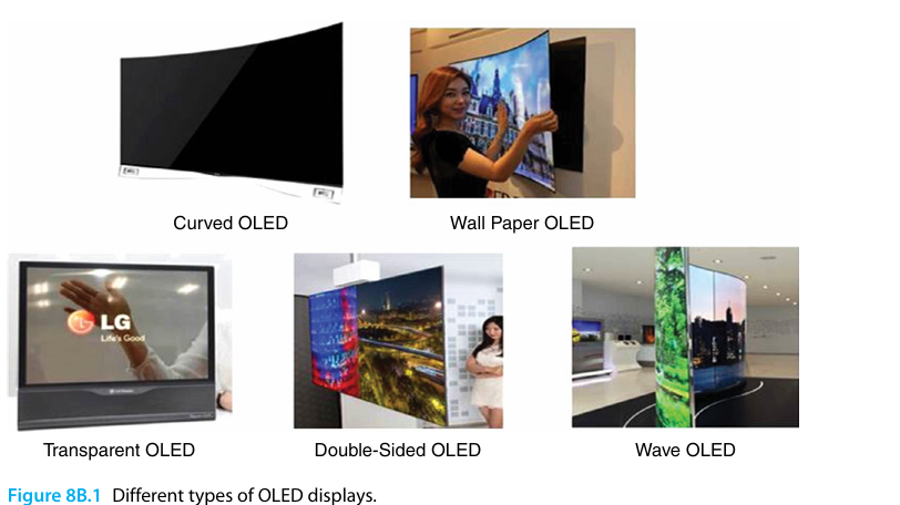
An OLED (Organic Light-Emitting Diode) is a type of LED whose emissive layer consists of an organic compound film that produces light when an electric current flows through it. This organic layer is sandwiched between two electrodes, at least one of which is typically transparent. The technology is widely found in everyday screens, including televisions, computer monitors, smartphones, and handheld game consoles. Additionally, the development of white OLEDs for solid-state lighting applications remains an active area of research. This is shown on Figure 1.

Applications
OLED technology is used across a broad range of products and industries. In consumer electronics, it is commonly found in smartphone screens, high-end televisions, computer monitors, and smartwatches. Its structural properties — thin form factor, flexibility, and the absence of a backlight — also make it suitable for more specialized applications such as automotive dashboards and instrument clusters.
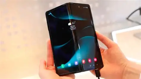
One notable area of development is the use of OLED in non-conventional display formats. Transparent OLED panels, which allow light to pass through when pixels are off, are used in applications such as retail signage and heads-up displays. Curved and flexible OLED screens have been integrated into various consumer devices, taking advantage of the technology's ability to be deposited on non-rigid substrates. Foldable displays, now present in a growing number of smartphones and tablets, also rely on flexible OLED panels to enable their form factor.
To understand in more detail what are the prevalent applications for screens, please check this page: Screen market review.
Working principle
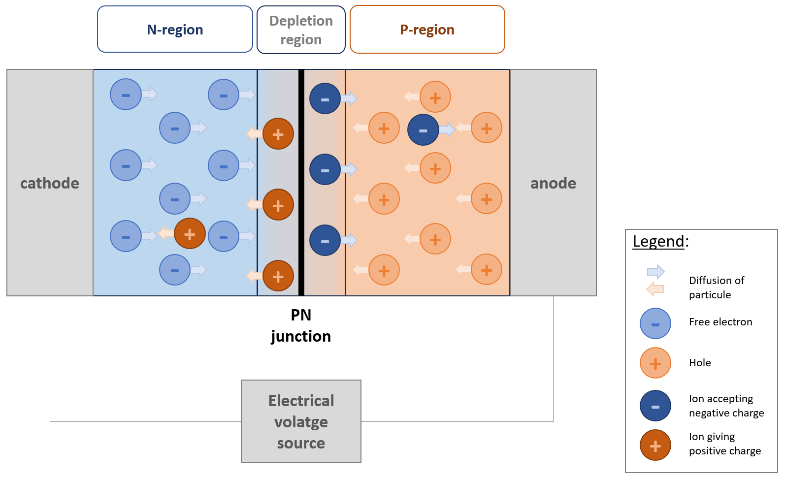
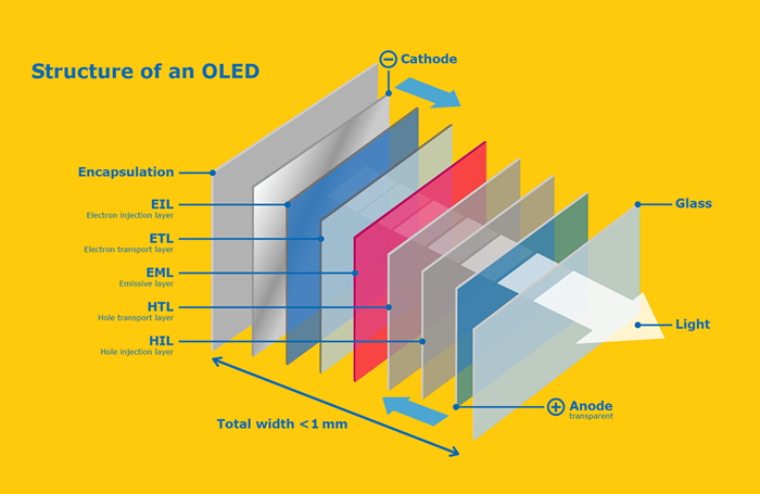
An OLED consists of a stack of organic layers sandwiched between an anode and a cathode. Usually there are at least 3 organic layers: a hole transport layer (HTL), an electron transport layer (ETL), and an emission layer (EML). When a specific electrical voltage is applied between the anode and the cathode, electrons (coming from the cathode through the ETL) and holes (coming from the anode through the HTL) are injected into the EML. Holes have a positive charge and are called “p particles”; electrons have a negative charge and are called “n particles”. Holes and electrons recombine in the EML - which is the p-n junction - forming excited electron-hole pairs as imaging in Figure 3. When a pair returns to its ground state, a photon is emitted: this is the electroluminescence.
The choice of materials constituting the ETL, HTL, and EML is fundamental in determining the OLED properties. To optimise the electron-hole recombination, and thus the OLED efficiency, the number of holes and the number of electrons must be equal in the EML. This is quite a challenge in organic semi-conductors because hole mobility is higher than electron mobility. The ETL often contains luminophores (especially in the small-molecule technology) which are molecules that emit light only in the presence of an electron-hole pair in a particular state (singlet). To improve the efficiency of the device, some transition materials can be added in the EML (this is the phosphorescent OLED technology) to allow light emission even if pairs are not in the singlet state.
Usually, luminophors are based on PPV (poly(p-phenylene vinylene) and on PFO (polyfluorene). One of the electrodes must be reflective and the other transparent, depending on the structure stack. The reflective one is mostly made of Al or Ag 1) , and the semi-transparent one is mostly made of Indium-Tin-Oxide (ITO) or Mg:Ag 2).
Technologies of light emission
OLED technology encompasses several distinct approaches to light emission, each relying on different materials or physical phenomena to generate light within the emissive layer.
- SMOLED (Small Molecules OLED)
The term OLED generally refers to small-molecule technology as it is the prevalent OLED technology. The light emission is produced by luminophores (in presence of electron-hole pairs), which are small molecules constituting the EML. The typical molecules used in SMOLEDs are organometallic chelates (e.g. Alq3 3)) or conjugated dendrimers.
- PLED (Polymer OLED)
In this technology, polymers are responsible for light emission (instead of luminophores in semiconductors). The PLED working principle is the same as in SMOLED, but the EML consists of polymers only. They are deposited by thin-film deposition.
- QD-OLED (Quantum-Dot OLED)
There are two types of QD displays: photo-emissive and electro-emissive. The main technology of QD display on the market is photo-emissive as the electro-emissive is only experimental to this date (2026). Hence, the term QD-OLED refers by default to photo-emissive QD-OLED, whose working principle is detailed below.
This technology is emerging in the market since 2023, developed mainly by Samsung4). It combines the SMOLED principle with the quantum-dot principle. A layer of SMOLED emits a monochromatic blue light, that is then converted by quantum dots (a thin layer of crystals placed above the blue OLED) to obtain the RGB spectrum. The size of the quantum dots determines the wavelength of the filtered rays and is therefore a dimensioning parameter.
- PhOLED (Phosphorescent OLED)
Phosphorescent OLEDs emit light by both fluorescence and phosphorescence phenomena. In classic OLEDs only fluorescence is observed thanks to electron-hole pairs (in a singlet state) de-excitation. By adding an organometallic complex into the EML, more electron-hole pairs are able to emit light (those in a triplet state) producing phosphorescence. The enhancement of the light emission efficiency by adding a material is called doping the EML.
- micro-OLED
This technology is used mainly for screens measuring in the order of a micrometer. Hence, OLEDs have to be smaller: that is where the real technological challenge lies. To date, this technology is still under development as only some wavelengths can be produced by micro-OLED
Types of OLED
OLED technology comes in a wide variety of implementations, differing in the way colors are generated, the direction in which light is emitted, and the method used to drive each pixel. The following sections cover the main distinctions across these three dimensions: structure types, structure stacks, and matrix types.
Structure types
OLED displays can be built using different architectures, each with its own approach to generating colour.
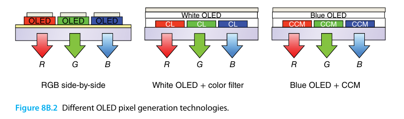
- WOLED (white OLED) with colour filters
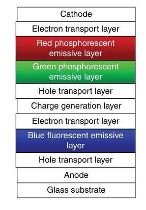
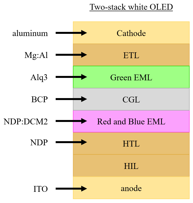
In this architecture, every sub-pixel emits white light. Colour is then obtained by passing that light through dedicated colour filters (red, green, blue). The intensity of each sub-pixel is individually controlled to achieve the desired colour and brightness. This approach is commonly used in large-screen applications such as TV panels, as it simplifies the manufacturing process. Several approaches exist to generate white light within a sub-pixel. Single-stack white OLEDs, which rely on a single emissive unit, tend to suffer from low efficiency and are therefore rarely used in practice. The most common solution is to stack two or three emissive units on top of each other, which significantly improves efficiency and brightness. The diagram below illustrates a two-stack white OLED architecture, combining red, green, and blue emissive layers :
- RGB side-by-side OLED
In this structure, each sub-pixel is an independent OLED emitting its own colour: red, green, or blue. By controlling the intensity of each sub-pixel individually, any colour can be reproduced with high accuracy. This approach offers excellent color purity and energy efficiency, since only the required colours are actually lit. It is widely used in smartphones and high-end displays.
- Blue OLED with colour converting materials
In this architecture, all sub-pixels start from a blue OLED emitter. Colour conversion materials such as quantum dots are then used to shift the blue light into red or green for the corresponding sub-pixels. This is typically based on QD-OLED technology. This approach combines the manufacturing simplicity of a single emitter type with the colour quality benefits of per-color emission.
- number of stacks
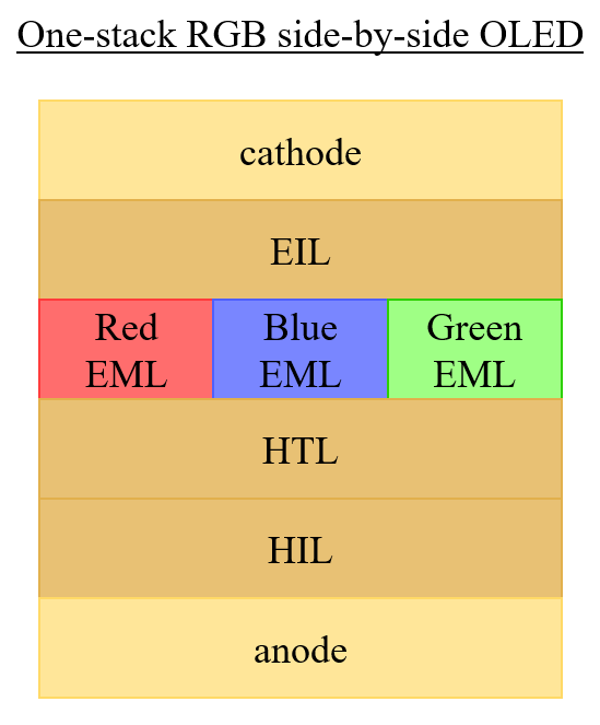
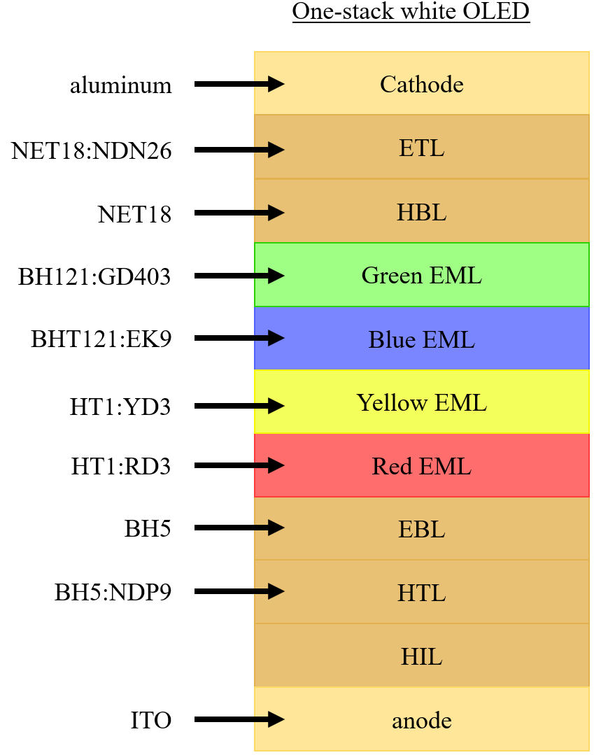
There are various stacks possible, depending on the display size or even on the display performance (brightness, power consumption). A one-stack OLED consists of the superposition of anode, HIL, HTL, EML, ETL, EIL, cathode. A two-stacked OLED consists of two one-stack OLED in series connection. The Figure 7 below set out the material layouts for these different options. The interconnection layer is called a charge generation layer (CGL) and plays both roles of anode and cathode. Figure 7 illustrates examples of stacks. The materials indicated with the arrows are abreviations for their scientific full name, their chemical formulas can be easily found in the literature. A material M1 doped with a material M2 is denoted as M1:M2.
Structure stacks
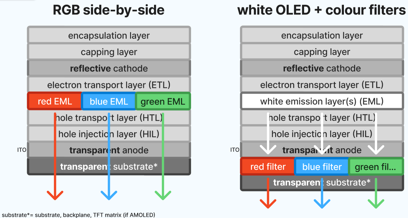
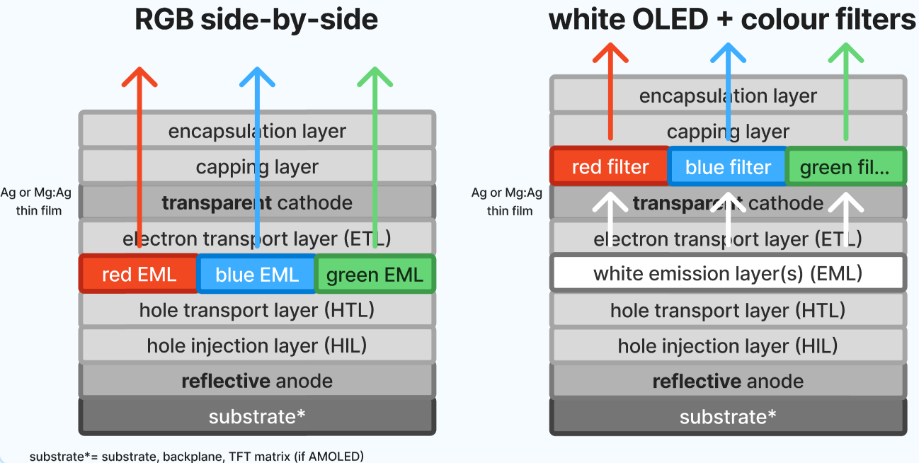
There are two types of OLED structure, depending on the light emission direction: the bottom-emission and the top-emission structures. In the bottom-emission structure, light is emitted through the anode and substrate whereas in the top-emission structure light is emitted through the cathode and encapsulation layer. Historically, bottom-emission is the first OLED structure that has emerged, but there are more and more OLED screens using the top-emission nowadays, especially for smaller screens.
BEOLED (bottom-emission OLED)
The characteristic of this structure is that light is directed from the emissive layer towards the anode and the substrate: they have to be transparent in the physical sense of the term (i.e. not interact with a wave, and hence not absorb light rays). Usually, the transparent electrode is made of ITO (indium-tin oxide) and the substrate is made of glass.
Because the emissive layer emits light in all directions, the cathode has to be made of a reflective material (e.g. silver) to redirect rays towards the anode.
The main disadvantage of the bottom-emission structure is that light has to pass through the pixel control circuit (the TFT matrix in the case of an AMOLED) that cannot be fully transparent. This implies a lower amount of light that can actually get out of the device. It is in this context that the top-emission structure emerged, to compensate for this drawback.
TEOLED (top-emission OLED)
In this structure, light is emitted from the emissive layer towards the cathode, it must therefore be transparent. Conversely, the anode must be reflective to redirect light towards the cathode. ITO is not a great fit for the cathode material due to technical constraints during the material deposition, and preferably a thin-film silver or magnesium-silver alloys is used. The cathode is however semi-transparent rather than transparent (some part of the incident rays are transmitted by the material and another part is reflected) which is not a problem if the material has great transmittance and conductivity.
Transparent OLED
This structure has two transparent electrodes: it is a combination of both bottom- and top-emission structures. This helps obtaining higher contrast levels and makes it particularly suitable for outdoor devices.
Matrix types
Another key distinction between OLED implementations lies in how each pixel is driven. There are two main approaches: the passive-matrix and the active-matrix driving methods, which differ in complexity, performance, and typical use cases.
- AMOLED (Active-Matrix OLED)
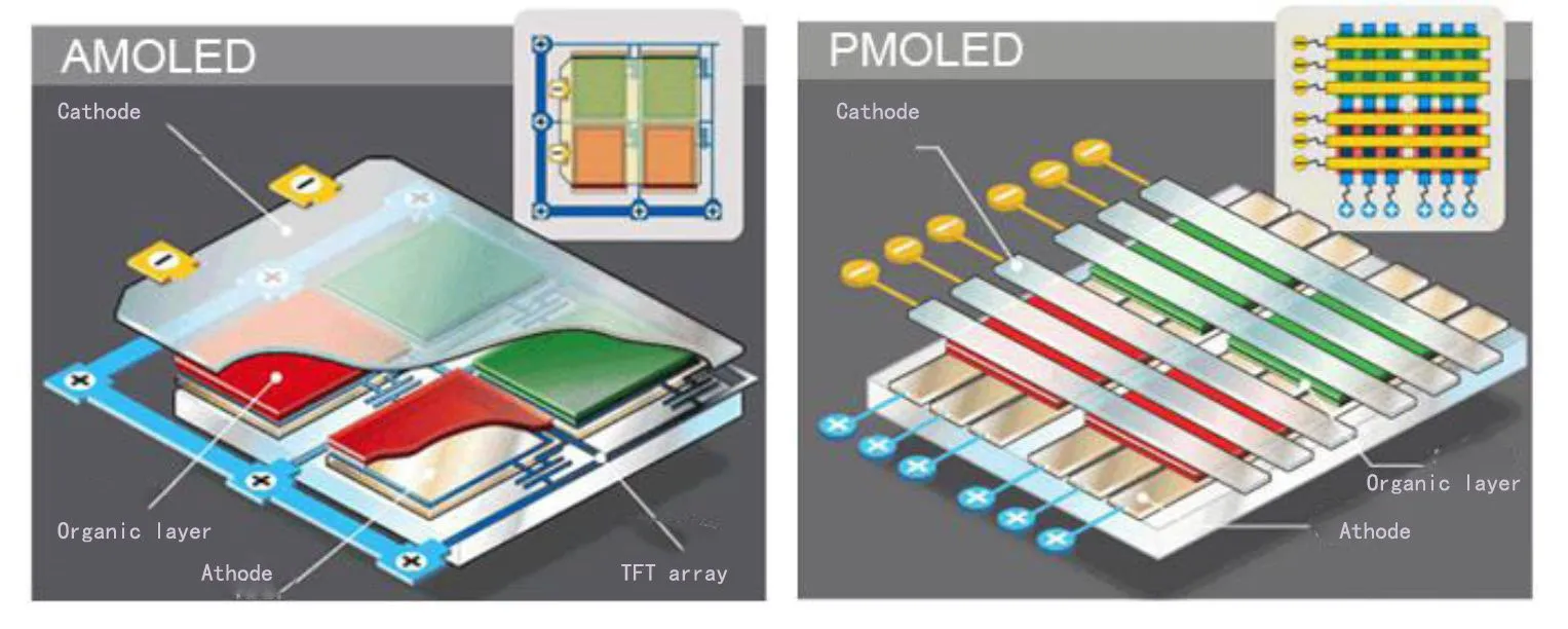
AMOLEDs include complete layers of cathode, organic components, and anode. The layers of anode consist of TFT (thin film transistors) in parallel to form a matrix, which helps switch each pixel to its on or off state as required hence, forming an image. When the pixels are not needed, they turn off or a black image on display occurs. This is the least power-consuming type and has quick refresh rates. They are commonly used in computer monitors, electronic signs or big TV screens. 9)
- PMOLED (Passive-Matrix OLED)
In a PMOLED display, pixels are driven row by row through a passive grid of conductors, without any dedicated transistor per pixel. This simpler architecture comes with inherent limitations: as the number of rows increases, brightness decreases, and a high-current driver IC is required to compensate. As a result, PMOLEDs are generally restricted to small screen sizes and lower resolutions. However, their fabrication process is significantly simpler and less costly than that of AMOLEDs, since no complex TFT backplane is needed. They are commonly found in small devices such as MP3 players and secondary displays 10)
Other topics
Types of rigidity: flexible vs. rigid OLED screens
Flexible OLED-based products aren’t always bendable or foldable 11). Flexibility is used to provide the display with a non-traditional form factor, but it is then bonded to a rigid glass cover in the product. e.g.: some smartphones (Samsung Galaxy Note, LG G Flex), some smartwatches (Apple Watch, LG watch urbane). The first smartphone using flexible AMOLED technology was introduced in 2013.
The difference in the manufacturing of flexible and rigid OLEDs lies in two processes steps: substrate and encapsulation (check this page for more information).