**This is an old revision of the document!**
Optical sensors
System Definition - Goal and scope
Definition
An optical sensor is a device that detects and converts light rays into electrical signals, allowing it to measure different physical properties such as distance, brightness, motion, temperature and pressure via optical methods.
The global optical sensor market was worth around \$25–28 billion in 2025 and is expected to reach approximately \$71.7 billion by 20351). This increase is directly linked to progress in automation, imaging and environmental monitoring technologies, as well as to the needs of the automotive, medical and industrial sectors.
What is it used for?
Thanks to the wide range of optical sensor technologies, a variety of applications are possible. These include consumer electronics, automotive camera systems, industrial machine vision and medical imaging etc.
| Application | Most common technologies | |
|---|---|---|
| Consumer Electronics | Smartphones, wearable electronics, and smart home devices. | Image sensor, Active ranging sensor modules |
| Industrial Automation and Robotics | Industrial automation, machine vision systems, and process monitoring equipment. | Photoelectric sensors, Image sensors, Fiber optic sensor, Infrared (IR) and Thermal Sensors |
| Automotive and Transportation | Advanced driver assistance systems and automotive safety technologies. | Active ranging sensor modules, Image sensors, Infrared (IR) and Thermal Sensors |
| Healthcare and Medical Devices | Medical monitoring devices, environmental detection systems, and smart infrastructure. | Infrared (IR) and Thermal Sensors, Fiber optic sensors, Photoelectric sensors |
| Biometrics and Security | Access control systems, document verification, surveillance and monitoring devices. | Image sensors, Infrared (IR) and Thermal Sensors |
| Aerospace and Defence | Surveillance, Reconnaissance & Intelligence systems, target tracking, navigation, and precision guidance. | Infrared (IR) and Thermal Sensors, Active ranging sensor modules, Image sensors |
| Energy and Environmental Monitoring | Monitor energy systems, measure air and water quality, detect pollutants and greenhouse gases. | Fiber optic sensors, Infrared (IR) and Thermal Sensors |
Are there different types/technologies?
The family of optical sensors is divided into different technology segments, which vary in terms of light sources, detection methods, and applications :
Image sensors
An image sensors convert light into electronic signals. The two most common types of image sensor are the charge-coupled device (CCD) and the active pixel sensor (CMOS).
CMOS sensors use pixel-level transistors to enable faster, more energy-efficient processing, while CCD sensors transfer charge across the chip to deliver superior image quality, but at the cost of slower speed and higher power consumption.
CMOS sensors are widely used in the consumer electronics sector. They are particularly used in mobile devices such as smartphones, tablets, and digital cameras.
Photoelectric sensors
Photoelectric sensors consist of a light emitter and a receiver. The light emitter uses a light-emitting diode (LED) to produce modulated pulses of light. The receivers contain photodiodes that convert the incoming light into electrical signals. These signals are then amplified and processed before being sent to the controller.
The three most common types of photoelectric sensor are through-beam, retro-reflective and diffuse reflection sensors2).
Photoelectric sensors are among the most common sensors used in industrial automation. They have many possible applications, including presence detection and safety protection. They can also offer relatively long operational distances for presence detection compared to other sensors.
Fiber optic sensors
A fiber optic sensor is a device that measures physical conditions using light transmitted through an optical fiber. « Optical signals are transmitted through a glass fiber. If external influences such as temperature, strain, pressure, or vibration change along the fiber or at its end, the measurable properties of the light change »3).
The glass fiber acts as the sensor. Therefore, it is electrically insulating and immune to electromagnetic interference and corrosion and is ideal for extreme environments. Fiber optic sensors are mainly used in the industrial, energy, and environmental monitoring sectors.
Active ranging sensor modules
An active ranging sensor module is a device that measures the distance to an object by sending out energy and analyzing the signal that comes back, using interferometry, time of flight, or triangulation methods4).
The most common types of active ranging sensor modules are ultrasonic sensors, LiDAR (Light Detection and Ranging) and radar sensors.
Infrared (IR) and Thermal Sensors
Infrared (IR) sensors and thermal sensors are generally considered part of the image sensor family, but they operate differently from standard visible-light image sensors. Infrared cameras primarily detect near-infrared light (close to the visible spectrum), while thermal imaging cameras detect mid- and far-infrared radiation (generated by the heat of objects)5).
They can also be applied to non-imaging sensors technology, such as passive infrared sensors (PIR) for motion detection, gas sensors, spectroscopy detectors and more.
If different types, what are the differences in terms of materials, process, use consumption?
Question à poser plutôt dans la page wiki d'une famille de capteur optique ex: Image sensors =⇒ Difference entre CMOS/CCD.
Is there a generic component that represents a family of components?
This study will focus on image sensors, which dominate the market for optical sensors6) and are used in many applications, including consumer electronics, automotive camera systems, industrial machine vision, and medical imaging.

How many sub-parts does the system consist of?
The main parts of a CMOS image sensor are the following:
- Sensor chip (wafer, node = 40-180nm): An array of photosensitive pixels, with Bayer pattern
- Wire bonds
- Package
- Cover glass
- Contact pads


Interesting sources :
Perimeter
What is included?
Focus on the optical sensor.
What is excluded?
Exclusion of other sensors like the distance sensor to adjust the focus. Exclusion of the rest of the image-processing system (PCB, controllers, etc.).
Exclusion of laser sensor and IR sensors. Not the focus for now
Functional unit and reference flows
What is the functional unit?
TBC
What are the reference flows?
TBC
State of the art: environmental impacts
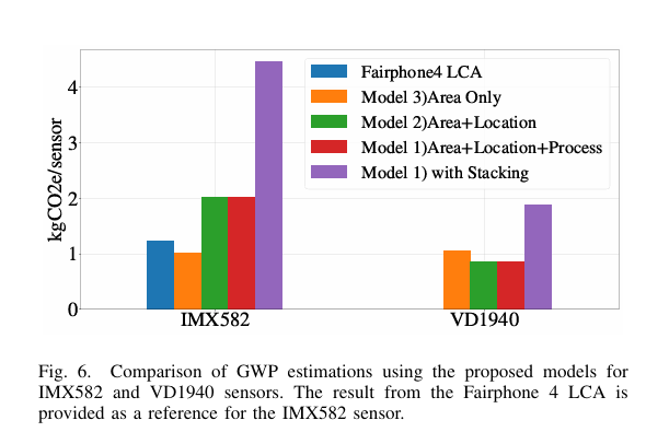
Streamlined Models of CMOS Image Sensors Carbon Impacts
This section summarises the information from Weppe and Al's 2024 study.7)
Methodology
Streamlined GHG emission model based on a linear relationship between silicon die surface area and Global Warming Potential (GWP), expressed in gCO2eq. The model follows:
$$G_{Fab} = \sum_{i=1}^{N} S_i \cdot (E_i \cdot T_{loc} +K_i)$$
GFab : Global Warming Potential (GWP) of the fabrication ( gCO2 eq)
Si : the surface of layer i
Ei : electrical energy consumption of layer i
Tloc : electrical carbon intensity of the location of fabrication
Ki : ancillary impact of the layer (infrastructure, factory, chemicals and raw materials)
The value of Ki and Ei are taken from 8)
Types of Technologies Covered (System Definition)
CMOS Image Sensor (CIS). Parameters affecting the scope: * CCD / CMOS * Mono / color sensor * Resolution → sensor size * Pixel size → sensor size * Stacking
Life Cycle Stages Covered
* Silicon die fabrication * Electricity consumption over lifespan
Fluxes Included in the Scope
Generic semiconductor data for a CIS. The following are excluded: * Lens * Color filter array * Other optical components
Main Results
Known hotspots : silicon die manufacturing, electricity consumption over lifespan, 2D/3D die stacking (factor 2 difference)
Limitations
Uses generic semiconductor data for a CIS, and therefore does not account for the specificities of CMOS image sensors, such as the lens, the color filter array, or other optical components.
Life Cycle - Inventory
⇒ Goal: Define state of the art on life cycle stages to be considered. * Samsung Electronics (South Korea, IDM) * OmniVision Technologies (US, fabless) * onsemi (US, IDM) * STMicroelectronics (CH, IDM)
Distribution and packaging
⇒ Goal: List the technical information needed for the LCI.
What are the packaging? Made of which materials?
TBC
Which are the transport modes?
TBC
What are the transport distances?
TBC
Use
⇒ Goal: List the technical information needed for the LCI.
What is the service lifespan? (durée d'utilisation)
TBC
Is there a reparation factor?
TBC
Is there sub-parts replacement?
TBC
Where is it used?
TBC
Who are the users?
TBC
Which + how much energy does it need?
TBC
Is there emissions from use?
TBC
End of life
⇒ Goal: List the technical information needed for the LCI.
What is the lifetime? (durée de vie)
TBC
Is it different from lifespan and why?
TBC
Is it refurbished? + Where?
TBC
Is it recyclable? Can it be dismantled? Which material can be separated? + Where and how?
TBC
Is it incinerated with energy recovery? Just incinerated? Buried? + Where?
TBC
Which part of waste can be considered as mismanaged (neither recycled, nor incinerated, nor buried)?
TBC
)
Next steps
⇒ Goal: List challenges and clarify priority areas for action