**This is an old revision of the document!**
Screen
Screens are electronic devices designed to display visual content by creating electronic pictures with illuminated pixels. Each pixel has three separate sub-pixels (red, blue, and green) that are individually controlled to create a color and brightness.
Screens are the main interface between people and machines in integrated devices, such as laptops, smartphones, and tablets, or as external displays for desktop computers. The screen's technology has progressed from large, bulky cathode ray tubes (CRTs) to thin, lightweight flat panel displays (FPDs) like LCDs and OLEDs.
System Definition - Goal and scope
Definition
A screen can be described as a graphical interface which converts electronic signals to a displayable form for the end-user. The technology consists of pixels that have been laid out in a matrix and can be controlled independently to display texts, images, or video sequences. Some of the properties of a screen include the type of technology (LCD, OLED), aspect ratio, dimension, and pixel resolution. In a life cycle assessment study of screen systems, all elements necessary for the performance of the screen will be included.
Function
Screens are mainly used to provide a visual connection between computer processing units and human beings. They come in integrated forms in television sets, mobile phones, and laptops.
Emissive technologies
There are several technologies that have been prominent in the development of the display industry. Here is a list of several screen technologies, summed up in the Figure 1 below. These technologies can be touch-sensitive or not, flexible or rigid, transparent or not.
- CRTs (Cathode Ray Tubes): They operate by generating an electron beam within a vacuum tube and projecting it onto a layer of phosphor materials. When these materials are struck by the electrons, they emit light through a process known as cathodoluminescence, thereby forming the image on the screen 1). This technology was widely used in televisions, computer monitors and oscilloscopes during the 20th century. It is an older technology and has now largely been replaced by flat-panel displays (LCD, OLED) due to its bulkiness, high energy consumption and limitations in terms of miniaturisation.
- LCDs (Liquid Crystal Displays): They use a backlight source whose rays pass through a layer of electrically controlled liquid crystals. Depending on their orientation, these crystals modify the passage of light through polarising filters, which allows the different colours and brightness levels of the image to be formed 2). Unlike emissive displays, LCD pixels do not directly produce light. The backlight is usually made of LEDs instead of earlier cold cathode fluorescent lamps. This technology is used in many products such as televisions, laptops, smartphones and measuring instruments. Widely industrialised from the 1990s onwards, it remains very widespread today thanks to its low energy consumption, compact size and relatively low manufacturing cost3).
- OLEDs (Organic Light Emitting Diodes): These screens are based on the electroluminescence of organic semiconductor materials, which emit light when an electric current passes through them 4). Unlike LCD screens, each pixel is self-illuminating and therefore no backlight is required: high contrast ratios and thinner screens can be obtained 5). However, OLED screens consume more power than LCDs in bright conditions as organic molecules need to be excited. Similarly, they consume less energy than LCDs in dark conditions as each pixel can be switched off completely. This technology is used in smartphones, televisions, smartwatches and high-end flexible screens. Increasingly popular since the 2000s, OLED is considered a newer technology than LCD and CRT screens.
- E-paper or Electronic Paper: E-paper (or electronic paper) screens work using small capsules containing charged particles that move under the influence of an electric field. By changing their position, these particles either brighten or darken certain areas of the screen by reflecting ambient light 6). This technology, used in e-readers, in certain digital labels and low-power devices, does not produce light but operates in reflective mode.
- Plasma Display (PDPs, Plasma Display Panels): They produce light by exciting an ionised gas enclosed in small cells. This excitation generates UV radiations which then stimulates fluorescent materials (luminophores) to produce visible light 7). This technology was mainly used in large-format TVs in the early 2000s and in some professional monitors, but is now considered obsolete, as LCD and OLED technologies are more energy-efficient and easier to miniaturise.

Transistor technologies
Display performance depends in part on the transistor technology used to drive the pixels. There are several technologies whose characteristics directly influence the optoelectronic performance of displays, including refresh rate, luminance, pixel density and energy efficiency.
- Amorphous silicon (a-Si): It is the most mature and widely used backplane technology due to its straightforward manufacturing and scalability to massive substrate sizes. It involves depositing an amorphous silicon film via plasma-enhanced chemical vapor deposition (PECVD), which is highly cost-effective. While it is excellent for general applications, a-Si has low electron mobility (around 0.5 to 1.0 cm²/Vs), limiting its use in ultra-high-resolution or high-refresh-rate displays 8).
- Indium-galium-zinc oxide (IGZO): IGZO, being a metal oxide semiconductor, represents a major leap in performance over a-Si. It offers 10 to 20 times higher mobility 9), enabling smaller transistors that increase pixel aperture ratios and allow for higher resolutions. One of IGZO's most unique properties is its extremely low off-state leakage current, which permits low-refresh-rate driving (as low as 1Hz) to save power during static images 10). It is highly compatible with existing a-Si manufacturing lines, making it a scalable solution for large 8K TVs and high-end monitors. While it is more sensitive to moisture and oxygen, leading to the need for advanced passivation layers 11), it is currently a leading backplane for both LCDs and large OLED TVs.
- Low-temperature polycrystalline silicon (LTPS): It is a high-performance backplane technology mainly used in premium smartphones and mobile devices. It is produced by using excimer laser annealing (ELA) to transform amorphous silicon into a highly organized crystalline structure. This results in very high electron mobility (often >100 cm²/Vs), allowing for much smaller transistors and the integration of complex circuits directly on the glass 12). This technology, called system on glass (SOG), helps manufacturers create ultra-thin bezels in modern smartphones. However, the laser process is expensive, complex, and difficult to scale to large TV-sized substrates with uniform quality 13).
- Low-temperature polycrystalline oxide (LTPO): It is an advanced hybrid backplane technology that combines LTPS and oxide TFT technologies on the same substrate. LTPS transistors handle fast switching and processing tasks, while oxide transistors are used for pixel driving because they consume very little power. This combination allows displays to adjust refresh rates dynamically, switching from very high refresh rates for gaming to extremely low refresh rates, such as 1 Hz, for power saving 14). As a result, LTPO displays can significantly improve battery life. The manufacturing process is more complicated and expensive because it requires more photolithography steps and precise temperature control 15). Currently, LTPO is used in flagship smartphones and smartwatches, where energy efficiency and display performance are especially important.
Components
Generic substrates of specialty glasses form the base for the layers of the display in practically all flat panel displays. The matrix of the thin film transistors (TFT) represents yet another universal family component that regulates each pixel in the active matrix.
An ordinary LCD assembly usually comprises several significant sub-assemblies, including the LCD panel, the backlight module, and the electronic controller.
The OLED assembly includes a substrate, a TFT matrix, an anode, multiple organic layers, a cathode, and an essential protective encapsulation layer. Ancillary sub-assemblies common to both families include the chassis, internal wiring, and stand. This is illustrated on Figure 2.

Screen market review
See the Screen market review dedicated page.
Perimeter
Included in the LCA
The scope of this life cycle assessment study involves the complete screen unit, encompassing the screen panel itself. This also extends back to upstream production processes such as the mining and refinement of materials used to create the screen, as well as the manufacturing of sub-units such as backlighting and the screen glass. Distribution is considered as part of the perimeter as it involves transport from the manufacturing facility to the end-user.
Excluded from the LCA
The housing, internal wiring, any cables, CPU of the computer and any accessories such as keyboards or mice are not included in the scope of many life cycle assessments for screens
Functional unit and reference flows
Functional Unit
The functional unit of this study is “ ? one rigid display panel without touchscreen”
Reference flow
The reference flow is one square meter of panel
State of the art: environmental impacts
State of the art in the environmental assessment of screen technology was once characterized by the evaluation of mature technologies such as CRTs, whereas the current cutting-edge of the screen is dominated by thin film technologies such as LCD, LED, and OLED. It aims to provide a scientific baseline that allows manufacturers to identify environmental “bottlenecks” and implement design-for-environment strategies early in the product development cycle.
Article 1: Environmental Effects of the Technology Transition from Liquid–Crystal Display (LCD) to Organic Light-Emitting Diode (OLED) Display from an E-Waste Management Perspective, Yeom & al. (2018)
This article has been published by Yeom JM & al. in 2018 19) and will be described below.
Methodology
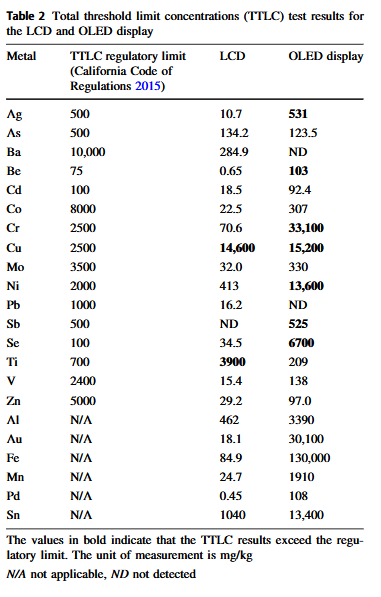
The study relies on two procedures from the United States of America and the state of California : the Toxicity Characteristics Leaching Procedure (TCLP) 20) and the Total Threshold Limiting Concentrations (TTLC) 21), which together test for a broad range of metals. Several impact assessment methods are used to estimate resource depletion potential as well as toxicity potentials (cancer, non-cancer, ecotoxicity) across different media (water, soil, air).
Types of Technologies Covered (System Definition)
Two small displays (approximately 60×60 mm) are compared: one OLED and one LCD. The study is therefore a technology-focused comparison of the material composition of these two display technologies.
Life Cycle Stages Covered
The study focuses exclusively on the end-of-life stage, assessing risks related to metal leaching and toxicity during disposal or recycling. Production, use, and transport phases are not covered.
Fluxes Included in the Scope
The scope covers the metal content of the displays, including: precious metals (gold, palladium, silver), heavy and potentially toxic metals (chromium, cadmium, arsenic, lead, beryllium, antimony, selenium, copper, iron, manganese, barium, titanium, zinc, tin). Energy flows, GHG emissions, and non-metallic materials are outside the scope.
Main Results
- The OLED display contains approximately 18 times more total metal mass than the LCD.
- The resource depletion potential of the OLED is 1,000 to 2,300 times higher, driven primarily by gold, followed by selenium, silver, palladium, tin, and antimony depending on the method used.
- Cancer potentials in water and soil are up to 600 times higher for the OLED, driven primarily by chromium; air cancer potential is 3 times higher due to cadmium and arsenic.
- Non-cancer potentials are 2–5 times higher for the OLED, linked mainly to arsenic and cadmium.
- Ecotoxicity is 40 times higher in air (driven by antimony) and 8–16 times higher in water and soil (driven by chromium) for the OLED.
- Palladium and antimony are classified as critical raw materials by the European Union, raising supply security concerns; beryllium, present at 235 times higher concentrations in the OLED, is also a critical raw material.
Limitations
- The study is based on two very small displays, which may not be representative of larger commercial screens.
- Only the end-of-life stage is analysed; impacts from production or use are not addressed.
- Non-metallic materials (plastics, glass, organic compounds in OLEDs) are outside the scope, providing only a partial picture of overall environmental impacts.
Article 2: Life cycle assessment of organic light emitting diode display as emerging materials and technology, Amasawa & al
This article has been published by Amasawa & al 22) and its content will be described below.
Methodology
Life Cycle Assessment (LCA) with the ISO 1404023) standard, and two criteria : Cumulative Energy Demand (CED) and Global Warming Potential (GWP) based on the IPCC 100-year framework 24)
Types of Technologies Covered (System Definition)
Functional unit: “One assembled 5-inch AMOLED display at the AMOLED manufacturing site in South Korea.”
The structure consists of:
- A TFT array substrate
- An OLED unit comprising six layers: anode (ITO), hole transport layer (HTL), emissive layer (EML), electron transport layer (ETL), electron injection layer (EIL), and cathode
- Packaging involving a cover glass and sealant (glass frit)
Life Cycle Stages Covered
The scope is a cradle-to-gate assessment. It includes:
- Raw material acquisition
- OLED fabrication (pre-treatment, organic/metal layer deposition via vacuum vapor deposition)
- Display assembly/packaging
- The use stage and disposal (end-of-life) are excluded from the system boundaries
Fluxes Included in the Scope
- Included: Specialty organic chemicals (e.g., Alq3, CuPc), sheet glass, ITO glass, metals (magnesium-silver targets), and electricity (reflecting the South Korean average grid mix)
- Excluded: Transistor patterning (omitted to focus on OLED-specific components), assembly of the smartphone with other parts, manufacturing equipment, and transportation of raw materials to the site
Main Results
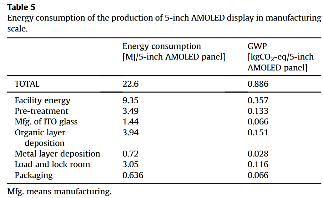
- Orders of Magnitude: The manufacturing of one 5-inch AMOLED display results in a CED of 22.6 MJ and a GWP of 0.886 kg CO2-eq
- Hot Spots: The facility energy is the largest contributor, accounting for 41.5% of the total impact. The organic layer deposition process is the second largest contributor
- Process vs. Material: Despite the complexity of specialty chemicals, their synthesis is not a significant contributor; instead, nearly 80% of the impact within the organic layer deposition stage comes from the vacuum vapor deposition process itself
- Comparison: AMOLED displays exhibited a lower GWP for materials when compared to similar-sized Liquid Crystal Displays (LCD)
Limitations
- Chemical LCI Gaps: The methodology for specialty chemicals does not yet account for waste or byproducts generated during their production, which could influence the true energy requirements
- Scaling Assumptions: The “Rule of Square Root” assumes production cost is linearly proportional to energy consumption, which may underestimate actual energy use by ignoring costs related to labor or equipment amortization
- Scope Exclusions: By excluding manufacturing equipment and transportation, the study may not capture the full environmental footprint
- Data Specificity: The results are specific to the South Korean electricity mix and a 5-inch display size, potentially limiting generalizability to other regions or form factors
Life Cycle - Inventory
⇒ Goal: Define state of the art on life cycle stages to be considered.
Database and tools
Existing data
To be added
Raw materials
To be added
Manufacturing
The main stages of screen manufacturing are:
- substrate fabrication and preparation
- array process (with colour filter – optional
- liquid cirstal cells (for LCD screens) or organic materials (for OLED screens)
- module process (only for LCD screens)
- overcoat and encapsulation process (only for OLED screens)
- assembly and testings
The description of manufacturing processes for both LCD and OLED screens is detailed in the manufacturing processes of screens page.
Distribution and packaging
To be added (types and materials of packaging, transport modes and distances)
Use
Out of scope
End of life
Out of scope
Next steps
What do we know we don't know? (The process technologies and yields must have improved in the past years)
What are the identified challenges? (Almost no data at all)
What paths/ideas should be explored?